SLVSC85C August 2013 – May 2015 TPS65279
PRODUCTION DATA.
- 1 Features
- 2 Applications
- 3 Description
- 4 Revision History
- 5 Description (continued)
- 6 Pin Configuration and Functions
- 7 Specifications
-
8 Detailed Description
- 8.1 Overview
- 8.2 Functional Block Diagram
- 8.3
Feature Description
- 8.3.1 Enable and Adjusting Undervoltage Lockout (UVLO)
- 8.3.2 Adjustable Switching Frequency and Synchronization
- 8.3.3 Soft-Start Time
- 8.3.4 Out-of-Phase Operation
- 8.3.5 Output Overvoltage Protection (OVP)
- 8.3.6 Bootstrap Voltage (BOOT) and Low Dropout Operation
- 8.3.7 Overcurrent Protection
- 8.3.8 Current Sharing Operation
- 8.3.9 Thermal Shutdown
- 8.4 Device Functional Modes
- 9 Application and Implementation
- 10Power Supply Recommendations
- 11Layout
- 12Device and Documentation Support
- 13Mechanical, Packaging, and Orderable Information
Package Options
Mechanical Data (Package|Pins)
Thermal pad, mechanical data (Package|Pins)
Orderable Information
6 Pin Configuration and Functions
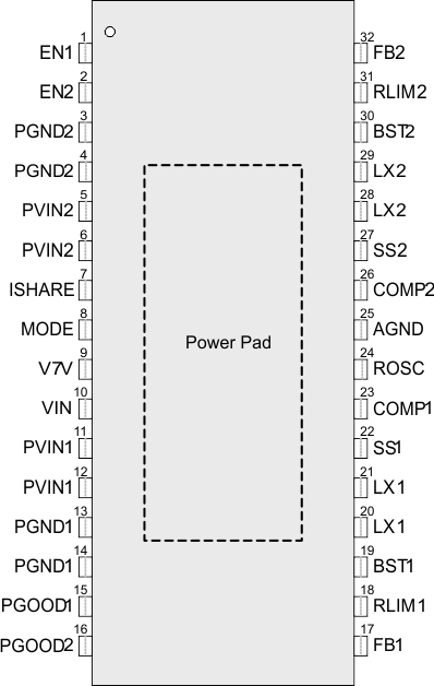
DAP Package
32-Pin HTSSOP
Top View

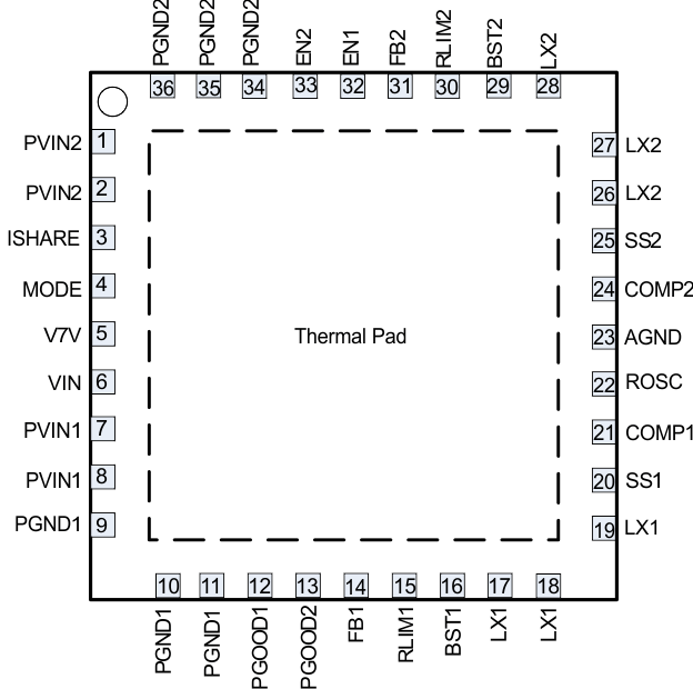
RHH Package
36-Pin VQFN
Top View

Pin Functions
| PIN | DESCRIPTION | ||
|---|---|---|---|
| NAME | HTSSOP | VQFN | |
| EN1, EN2 | 1, 2 | 32, 33 | Enable pin. Adjust the input under-voltage lockout with two resistors. |
| PGND2 | 3, 4 | 34, 35, 36 | Power ground of buck2, place the input capacitor’s ground pin as close as possible to this pin. |
| PVIN2 | 5, 6 | 1, 2 | Power input. Input power supply to the power switches of the power converter 2. |
| ISHARE | 7 | 3 | Logic pin to configure current sharing mode, tie to high to parallel two buck converters, in current sharing mode, buck1 will be used; tie to low to run in separate mode. |
| MODE | 8 | 4 | Connecting this pin to ground, the buck converter forces a continuous current mode (CCM) operation. Connecting this pin to V7V, the buck converter automatically operates in pulse skipping mode (PSM) at light load condition to save the power. |
| V7V | 9 | 5 | Internal low-drop linear regulator (LDO) output to power internal driver and control circuits. Decouple this pin to power ground with a minimum 1-µF ceramic capacitor. Output regulates to typical 6.3 V for optimal conduction on-resistances of internal power MOSFETs. In PCB design, the power ground and analog ground should have one-point common connection at the (-) terminal of V7V bypass capacitor. If VIN is lower than 6.3 V, V7V will be slightly lower than VIN. |
| VIN | 10 | 6 | Power supply of the internal LDO and controllers |
| PVIN1 | 11, 12 | 7, 8 | Power input. Input power supply to the power switches of the power converter 1. |
| PGND1 | 13, 14 | 9, 10, 11 | Power ground of buck1, place the input capacitor’s ground pin as close as possible to this pin. |
| PGOOD1 | 15 | 12 | Power Good pin for buck1, open drain output, when output is within range, output high impedance, a 100-kΩ resistor is recommended to connect to this pin. |
| PGOOD2 | 16 | 13 | Power Good pin for buck2, open drain output, when output is within range, output high impedance, a 100-kΩ resistor is recommended to connect to this pin. |
| FB1 | 17 | 14 | Feedback sensing pin for buck1 output voltage. Connect this pin to the resistor divider of buck1 output. The feedback reference voltage is 0.6 V ±1%. |
| RLIM1 | 18 | 15 | Current limit threshold set pin for buck1, connect a resistor between this pin to GND to set the OCP. |
| BST1 | 19 | 16 | Add a bootstrap capacitor between BST1 and LX1. The voltage on this capacitor carries the gate drive voltage for the high-side MOSFET. |
| LX1 | 20, 21 | 17, 18, 19 | Switching node of buck1 |
| SS1 | 22, 27 | 20, 25 | Soft-start and voltage tracking in buck1. An external capacitor connected to this pin sets the internal voltage reference rise time. Since the voltage on this pin overrides the internal reference, it can be used for tracking and sequencing. In current sharing application, this pin serves as the soft-start pin. |
| COMP1 | 23 | 21 | Error amplifier output and loop compensation pin for buck1. Connect frequency compensation to this pin; In current sharing application, this pin serves as the compensation pin. |
| ROSC | 24 | 22 | Oscillator frequency programmable pin. Connect an external resistor to set the switching frequency. When connected to an external clock, the internal oscillator synchronizes to the external clock. |
| AGND | 25 | 23 | Analog ground of the controllers |
| COMP2 | 26 | 24 | Error amplifier output and loop compensation pin for buck2. Connect frequency compensation to this pin. In current sharing application, float this pin. |
| SS2 | 27 | 25 | Soft-start and voltage tracking in buck2. An external capacitor connected to this pin sets the internal voltage reference rise time. Since the voltage on this pin overrides the internal reference, it can be used for tracking and power sequencing. In current sharing application, float this pin. |
| LX2 | 28, 29 | 26, 27, 28 | Switching nodes |
| BST2 | 30 | 29 | Add a bootstrap capacitor between BST2 and LX2. The voltage on this capacitor carries the gate drive voltage for the high-side MOSFET of buck2. |
| RLIM2 | 31 | 30 | Current limit threshold set pin for buck2, connect a resistor between this pin to GND to set the OCP. |
| FB2 | 32 | 31 | Feedback sensing pin for buck2 output voltage. Connect this pin to the resistor divider of buck2 output. The feedback reference voltage is 0.6 V ±1%. In current sharing mode, connect this pin to ground. |
| Exposed Thermal Pad | 33 | 37 | Exposed thermal pad of the package. Connect to the power ground. Always solder thermal pad to the board, and have as many vias as possible on the PCB to enhance power dissipation. There is no electric signal down bonded to the thermal pad inside the IC package. |