SLVSC27D July   2013  – October 2016 TPS65631W

PRODUCTION DATA.  

  1. Features
  2. Applications
  3. Description
  4. Simplified Schematic
  5. Revision History
  6. Pin Configuration and Functions
  7. Specifications
    1. 7.1 Absolute Maximum Ratings
    2. 7.2 ESD Ratings
    3. 7.3 Recommended Operating Conditions
    4. 7.4 Thermal Information
    5. 7.5 Electrical Characteristics
    6. 7.6 Timing Requirements
    7. 7.7 Typical Characteristics
  8. Detailed Description
    1. 8.1 Overview
    2. 8.2 Functional Block Diagram
    3. 8.3 Feature Description
      1. 8.3.1 Boost Converter
      2. 8.3.2 Inverting Buck-Boost Converter
      3. 8.3.3 Soft-Start and Start-Up Sequence
      4. 8.3.4 Enable (CTRL)
      5. 8.3.5 Undervoltage Lockout
      6. 8.3.6 Short Circuit Protection
        1. 8.3.6.1 Short-Circuits During Normal Operation
        2. 8.3.6.2 Short-Circuits During Start-Up
      7. 8.3.7 Thermal Shutdown
    4. 8.4 Device Functional Modes
      1. 8.4.1 Operation with VI < 2.9 V
      2. 8.4.2 Operation with VI ≈ VPOS (Diode Mode)
      3. 8.4.3 Operation with CTRL
    5. 8.5 Programming
      1. 8.5.1 Programming VNEG
  9. Applications and Implementation
    1. 9.1 Application Information
    2. 9.2 Typical Application
      1. 9.2.1 Design Requirements
      2. 9.2.2 Detailed Design Procedure
        1. 9.2.2.1 Inductor Selection
        2. 9.2.2.2 Capacitor Selection
        3. 9.2.2.3 Stability
      3. 9.2.3 Application Curves
  10. 10Power Supply Recommendations
  11. 11Layout
    1. 11.1 Layout Guidelines
    2. 11.2 Layout Example
  12. 12Device and Documentation Support
    1. 12.1 Device Support
      1. 12.1.1 Third-Party Products Disclaimer
    2. 12.2 Receiving Notification of Documentation Updates
    3. 12.3 Community Resources
    4. 12.4 Trademarks
    5. 12.5 Electrostatic Discharge Caution
    6. 12.6 Glossary
  13. 13Mechanical, Packaging, and Orderable Information

Package Options

Mechanical Data (Package|Pins)
Thermal pad, mechanical data (Package|Pins)
Orderable Information

6 Pin Configuration and Functions

SON (DSK) PACKAGE
10-PINS
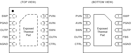
TPS65631W PinOut_TPS65631W.gif

Pin Functions

NAME NO. I/O DESCRIPTION
AGND 5 Analog ground.
AVIN 9 Input supply voltage for internal analog circuits (both converters).
CTRL 6 I Control pin. Combined device enable and inverting buck-boost converter output voltage programming pin.
FBS 4 I Feedback sense pin of the boost converter output voltage.
PGND 2 Power ground of the boost converter.
PVIN 10 Input supply voltage pin for the inverting buck-boost converter.
SWN 8 O Switch pin of the inverting buck-boost converter.
SWP 1 O Switch pin of the boost converter.
OUTN 7 O Rectifier pin of the inverting buck-boost converter.
OUTP 3 O Rectifier pin of the boost converter.
Exposed Thermal Pad Connect this pad to AGND and PGND.