SWCS071C August 2012 – August 2017
PRODUCTION DATA.
- 1 Device Overview
- 2 Revision History
- 3 Default Settings
- 4 Pin Configuration and Functions
-
5 Specifications
- 5.1 Absolute Maximum Ratings
- 5.2 ESD Ratings
- 5.3 Recommended Operating Conditions
- 5.4 Thermal Characteristics
- 5.5 Electrical Characteristics - DCDC1, DCDC2, and DCDC3
- 5.6 Electrical Characteristics - DCDC4
- 5.7 Electrical Characteristics - LDOs
- 5.8 Electrical Characteristics - Digital Inputs, Digital Outputs
- 5.9 Electrical Characteristics - VMON Voltage Monitor, VDDIO, Undervoltage Lockout (UVLO), and LDOAO
- 5.10 Electrical Characteristics - Load Switch
- 5.11 Electrical Characteristics - LED Drivers
- 5.12 Electrical Characteristics - Thermal Monitoring and Shutdown
- 5.13 Electrical Characteristics - 32-kHz RC Clock
- 5.14 SPI Interface Timing Requirements
- 5.15 I2C Interface Timing Requirements
- 5.16 Typical Characteristics
- 6 Parameter Measurement Information
-
7 Detailed Description
- 7.1 Overview
- 7.2 Functional Block Diagram
- 7.3 Linear Regulators
- 7.4 Step-Down Converters
- 7.5 GPIOs
- 7.6 Power State Machine
- 7.7 Transition Conditions
- 7.8 Implementation of Internal Power-Up and Power-Down Sequencing
- 7.9 EN1, EN2, EN3, EN4, Resources Control
- 7.10 SLEEP State Control
- 7.11 Registers SET_OFF, KEEP_ON and DEF_VOLT Used in SLEEP State; CONFIG2 = 1
- 7.12 Registers SET_OFF, KEEP_ON and DEF_VOLT Used for Resources Assigned to an External Enable Pin; CONFIG2 = 1
- 7.13 Registers SET_OFF, KEEP_ON and DEF_VOLT for Resources Assigned to Pins PWR_REQ, CLK_REQ1 and CLK_REQ2; CONFIG2 = 0
- 7.14 Voltage Scaling Interface Control Using _OP and _AVS Registers with I2C or SPI Interface
- 7.15 Voltage Scaling Using the VCON Decoder on Pins VCON_PWM and VCON_CLK
- 7.16 Configuration Pins CONFIG1, CONFIG2 and DEF_SPI_I2C-GPIO
- 7.17 VDDIO Voltage for Push-Pull Output Stages
- 7.18 Digital Signal Summary
- 7.19 TPS659121 On/Off Operation With E450, E500
- 7.20 TPS659122 On/Off Operation for CONFIG1=HIGH
- 7.21 TPS659122 On/Off Operation for CONFIG1=LOW
- 7.22 Interfaces
- 7.23 Serial Peripheral Interface
- 7.24 I2C Interface
- 7.25 Thermal Monitoring and Shutdown
- 7.26 Load Switch
- 7.27 LED Driver
- 7.28
Memory
- 7.28.1 Register Format
- 7.28.2
Register Descriptions
- 7.28.2.1
DCDC Registers
- 7.28.2.1.1 DCDC1_CTRL (00h)
- 7.28.2.1.2 DCDC2_CTRL (01h)
- 7.28.2.1.3 DCDC3_CTRL (02h)
- 7.28.2.1.4 DCDC4_CTRL (03h)
- 7.28.2.1.5 DCDC1_OP (04h)
- 7.28.2.1.6 DCDC1_AVS (05h)
- 7.28.2.1.7 DCDC1_LIMIT (06h)
- 7.28.2.1.8 DCDC2_OP (07h)
- 7.28.2.1.9 DCDC2_AVS (08h)
- 7.28.2.1.10 DCDC2_LIMIT (09h)
- 7.28.2.1.11 DCDC3_OP (0Ah)
- 7.28.2.1.12 DCDC3_AVS (0Bh)
- 7.28.2.1.13 DCDC3_LIMIT (0Ch)
- 7.28.2.1.14 DCDC4_OP (0Dh)
- 7.28.2.1.15 DCDC4_AVS (0Eh)
- 7.28.2.1.16 DCDC4_LIMIT (0Fh)
- 7.28.2.1.17 VDCDCx Range Settings
- 7.28.2.1.18 DCDCx Voltage Settings
- 7.28.2.2
LDO Registers
- 7.28.2.2.1 LDO1_OP (10h)
- 7.28.2.2.2 LDO1_AVS (11h)
- 7.28.2.2.3 LDO1_LIMIT (12h)
- 7.28.2.2.4 LDO2_OP (13h)
- 7.28.2.2.5 LDO2_AVS (14h)
- 7.28.2.2.6 LDO2_LIMIT (15h)
- 7.28.2.2.7 LDO3_OP (16h)
- 7.28.2.2.8 LDO3_AVS (17h)
- 7.28.2.2.9 LDO3_LIMIT (18h)
- 7.28.2.2.10 LDO4_OP (19h)
- 7.28.2.2.11 LDO4_AVS (1Ah)
- 7.28.2.2.12 LDO4_LIMIT (1Bh)
- 7.28.2.2.13 LDO5 (1Ch)
- 7.28.2.2.14 LDO6 (1Dh)
- 7.28.2.2.15 LDO7 (1Eh)
- 7.28.2.2.16 LDO8 (1Fh)
- 7.28.2.2.17 LDO9 (20h)
- 7.28.2.2.18 LDO10 (21h)
- 7.28.2.3 LDO Voltage Settings
- 7.28.2.4
DEVCTRL Registers
- 7.28.2.4.1 THRM_REG (22h)
- 7.28.2.4.2 CLK32KOUT (23h)
- 7.28.2.4.3 DEVCTRL (24h)
- 7.28.2.4.4 DEVCTRL2 (25h)
- 7.28.2.4.5 I2C_SPI_CFG (26h)
- 7.28.2.4.6 KEEP_ON1 (27h)
- 7.28.2.4.7 KEEP_ON2 (28h)
- 7.28.2.4.8 SET_OFF1 (29h)
- 7.28.2.4.9 SET_OFF2 (2Ah)
- 7.28.2.4.10 DEF_VOLT (2Bh)
- 7.28.2.4.11 LDO Sleep Mode Behavior
- 7.28.2.4.12 DEF_VOLT_MAPPING (2Ch)
- 7.28.2.4.13 DISCHARGE1 (2Dh)
- 7.28.2.4.14 DISCHARGE2 (2Eh)
- 7.28.2.4.15 EN1_SET1 (2Fh)
- 7.28.2.4.16 EN1_SET2 (30h)
- 7.28.2.4.17 EN2_SET1 (31h)
- 7.28.2.4.18 EN2_SET2 (32h)
- 7.28.2.4.19 EN3_SET1 (33h)
- 7.28.2.4.20 EN3_SET2 (34h)
- 7.28.2.4.21 EN4_SET1 (35h)
- 7.28.2.4.22 EN4_SET2 (36h)
- 7.28.2.4.23 PGOOD (37h)
- 7.28.2.4.24 PGOOD2 (38h)
- 7.28.2.4.25 INT_STS (39h)
- 7.28.2.4.26 INT_MSK (3Ah)
- 7.28.2.4.27 INT_STS2 (3Bh)
- 7.28.2.4.28 INT_MSK2 (3Ch)
- 7.28.2.4.29 INT_STS3 (3Dh)
- 7.28.2.4.30 INT_MSK3 (3Eh)
- 7.28.2.4.31 INT_STS4 (3Fh)
- 7.28.2.4.32 INT_MSK4 (40h)
- 7.28.2.4.33 GPIO1 (41h)
- 7.28.2.4.34 GPIO2 (42h)
- 7.28.2.4.35 GPIO3 (43h)
- 7.28.2.4.36 GPIO4 (44h)
- 7.28.2.4.37 GPIO5 (45h)
- 7.28.2.4.38 VMON (46h)
- 7.28.2.4.39 LEDA_CTRL1 (47h)
- 7.28.2.4.40 LEDA_CTRL2 (48h)
- 7.28.2.4.41 LEDA_CTRL3 (49h)
- 7.28.2.4.42 LEDA_CTRL4 (4Ah)
- 7.28.2.4.43 LEDA_CTRL5 (4Bh)
- 7.28.2.4.44 LEDA_CTRL6 (4Ch)
- 7.28.2.4.45 LEDA_CTRL7 (4Dh)
- 7.28.2.4.46 LEDA_CTRL8 (4Eh)
- 7.28.2.4.47 LEDB_CTRL1 (4Fh)
- 7.28.2.4.48 LEDB_CTRL2 (50h)
- 7.28.2.4.49 LEDB_CTRL3 (51h)
- 7.28.2.4.50 LEDB_CTRL4 (52h)
- 7.28.2.4.51 LEDB_CTRL5 (53h)
- 7.28.2.4.52 LEDB_CTRL6 (54h)
- 7.28.2.4.53 LEDB_CTRL7 (55h)
- 7.28.2.4.54 LEDB_CTRL8 (56h)
- 7.28.2.4.55 LEDC_CTRL1 (57h)
- 7.28.2.4.56 LEDC_CTRL2 (58h)
- 7.28.2.4.57 LEDC_CTRL3 (59h)
- 7.28.2.4.58 LED_CTRL4 (5Ah)
- 7.28.2.4.59 LEDC_CTRL5 (5Bh)
- 7.28.2.4.60 LEDC_CTRL6 (5Ch)
- 7.28.2.4.61 LEDC_CTRL7 (5Dh)
- 7.28.2.4.62 LEDC_CTRL8 (5Eh)
- 7.28.2.4.63 LED_RAMP_UP_TIME (5Fh)
- 7.28.2.4.64 LED_RAMP_DOWN_TIME (60h)
- 7.28.2.4.65 LED_SEQ_EN (61h)
- 7.28.2.4.66 LEDx DC Current
- 7.28.2.4.67 LOADSWITCH (62h)
- 7.28.2.4.68 SPARE (63h)
- 7.28.2.4.69 VERNUM (64h)
- 7.28.2.1
DCDC Registers
- 8 Applications, Implementation, and Layout
- 9 Device and Documentation Support
- 10Mechanical, Packaging, and Orderable Information
Package Options
Mechanical Data (Package|Pins)
- YFF|81
Thermal pad, mechanical data (Package|Pins)
Orderable Information
8 Applications, Implementation, and Layout
NOTE
Information in the following applications sections is not part of the TI component specification, and TI does not warrant its accuracy or completeness. TI’s customers are responsible for determining suitability of components for their purposes. Customers should validate and test their design implementation to confirm system functionality.
8.1 Application Information
The TPS65912 device is an integrated power-management integrated circuit (PMIC) that comes in an 81- pin, 0.4-mm pitch, DSBGA package. This device was designed for personal electronic, industrial, and communication applications and is dedicated to designs powered from a 5-V input supply that require multiple power rails. The device provides four step-down converters along with an interface to control ten external LDO regulators. The device can support a variety of different processors and applications. The step-down converters can also support dynamic voltage scaling through a dedicated I2C interface to provide optimum power savings. In addition to the power resources, the device contains an embedded power controller (EPC) to manage the power sequencing requirements of systems. The power sequencing is programmable through OTP. The device also contains five configurable GPIOs, a real-time clock module, and three LED outputs. The following sections provide the typical application use-case with the recommended external components and layout guidelines.
8.2 Typical Application
8.2.1 DC-DC Converters
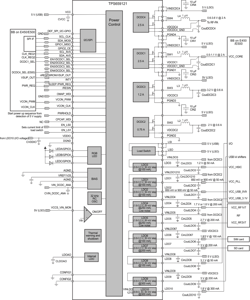 Figure 8-1 5-V USB Host Connections for E450 and E500 Platforms
8.2.1.1 Design Requirements
For a typical application shown in Figure 8-1, Table 8-1 lists the key design parameters of the power resources.
Table 8-1 Design Parameters
| DESIGN PARAMETER | VALUE |
|---|---|
| Supply voltage | 2.7 V to 5.5 V |
| Switching frequency | Up to 3.5 MHz |
| DCDC1 voltage | 1.1 V |
| DCDC1 current | Up to 2.5 A |
| DCDC2 voltage | 2.0 V |
| DCDC2 current | Up to 0.75 A |
| DCDC3 voltage | 3.2 V |
| DCDC3 current | Up to 1.6 A |
| DCDC4 voltage | 3.6 V |
| DCDC4 current | Up to 2.5 A |
| LDO1 voltage | 850 mV or 900 mV |
| LDO1 current | Up to 100 mA |
| LDO2 voltage | 850 mV or 900 mV |
| LDO2 current | Up to 100 mA |
| LDO3 voltage | 1.2 V |
| LDO3 current | Up to 100 mA |
| LDO4 voltage | 1.7 V or 1.8 V |
| LDO4 current | Up to 250 mA |
| LDO5 voltage | 2.7 V |
| LDO5 current | Up to 250 mA |
| LDO6 voltage | 1.8 V or 3.0 V |
| LDO6 current | Up to 100 mA |
| LDO7 voltage | 3.0 V |
| LDO7 current | Up to 200 mA |
| LDO8 voltage | 3.1 V |
| LDO8 current | Up to 100 mA |
| LDO9 voltage | 3.0 V |
| LDO9 current | Up to 300 mA |
| LDO10 voltage | 1.8 V |
| LDO10 current | Up to 300 mA |
8.2.1.2 Detailed Design Procedure
Table 8-2 lists the recommended external components.
Table 8-2 Recommended External Components
| REFERENCE COMPONENTS | COMPONENT(1) | MANUFACTURER | PART NUMBER | VALUE | EIA SIZE CODE(4) | SIZE (mm) | MASS PRODUCTION(2) |
|---|---|---|---|---|---|---|---|
| INPUT POWER SUPPLIES EXTERNAL COMPONENTS | |||||||
| CVCC, CVIN_DCDC_ANA, LDOAO | Power input capacitors | Murata | GRM188R71A225KE15 | 2.2 µF, 10V | 0603 | 1.6 × 0.8 × 0.8 | Available(3) |
| CVDDIO | I/O input capacitor | Murata | GRM188R60J475KE19 | 4.7 µF, 6.3V | 0603 | 1.6 × 0.8 × 0.8 | Available(3) |
| RGB LED EXTERNAL COMPONENTS | |||||||
| LEDA | Yellow LED | Lite On | LTST-C190YKT | 20mA, 2.1 V | 0603 | 1.6 × 0.8 × 0.8 | Available (3) |
| LEDB | Green LED | Lite On | LTST-C190GKT | 20mA, 2.1 V | 0603 | 1.6 × 0.8 × 0.8 | Available (3) |
| LEDC | Red LED | Lite On | LTST-C190CKT | 20mA, 2.1 V | 0603 | 1.6 × 0.8 × 0.8 | Available (3) |
| DCDC EXTERNAL COMPONENTS | |||||||
| CIN1, CIN2, CIN3, CIN4 | Input capacitor | Murata | GRM188R60J106ME47 | 10 µF, 6.3V | 0603 | 1.6 × 0.8 × 0.8 | Available (3) |
| CoutDCDC1, CoutDCDC4 | Output capacitor | Murata | GCM32ER70J476KE19 (Two capacitors per rail) | 10 µF, 6.3V | 0603 | 1.6 × 0.8 × 0.8 | Available (3) |
| CoutDCDC2, CoutDCDC3 | Output capacitor | Murata | GRM188R60J106ME47 | 10 µF, 6.3V | 0603 | 1.6 × 0.8 × 0.8 | Available (3) |
| L1, L2, L3, L4 | Inductor | Toko | 1239AS-H-1R0N=P2 | 1 µH | 2 × 2.5 | Available(3) | |
| LDO EXTERNAL COMPONENTS | |||||||
| CinLDO1210, CinLDO3, CinLDO67, CinLDO8, CinLDO9 | Input capacitor | Murata | GRM188R71A225KE15 | 2.2 µF, 10V | 0603 | 1.6 × 0.8 × 0.8 | Available(3) |
| CinLDO4, CinLDO5 | Input capacitor | Murata | GRM188R60J475KE19 | 4.7 µF, 6.3V | 0603 | 1.6 × 0.8 × 0.8 | Available(3) |
| CoutLDO3, CoutLDO1, CoutLDO2, CoutLDO6, CoutLDO7, CoutLDO8, CoutLDO9, CoutLDO10 | Output capacitor | Murata | GRM188R71A225KE15 | 2.2 µF, 10V | 0603 | 1.6 × 0.8 × 0.8 | Available(3) |
| CoutLDO4, CoutLDO5 | Output capacitor | Murata | GRM188R60J475KE19 | 4.7 µF, 6.3V | 0603 | 1.6 × 0.8 × 0.8 | Available(3) |
8.2.1.2.1 Output Filter Design (Inductor and Output Capacitor)
8.2.1.2.1.1 Inductor Selection
The step-down converters are designed to operate with small external components such as 1-μH output inductors. The values given under the recommended operating conditions include tolerances and saturation effects and must not be violated for stable operation. The selected inductor must be rated for its DC resistance and saturation current. The DC resistance of the inductance will influence directly the efficiency of the converter. Therefore an inductor with lowest DC resistance should be selected for highest efficiency.
Equation 1 can be used to calculate the maximum inductor current under static load conditions. The saturation current of the inductor should be rated higher than the maximum inductor current as calculated with Equation 1. This is recommended because during heavy load transient the inductor current will rise above the calculated value.

where
- ΔIL = Peak-to-peak inductor ripple current
- L = Inductor value
- f = Switching frequency

where
- ILmax = Maximum inductor current
The highest inductor current will occur at maximum Vin.
Open core inductors have a soft saturation characteristic and they can usually handle higher inductor currents versus a comparable shielded inductor.
A more conservative approach is to select the inductor current rating just for the maximum switch current of the corresponding converter. It must be considered, that the core material from inductor to inductor differs and will have an impact on the efficiency especially at high switching frequencies.
Refer to Table 8-3 and the typical applications for possible inductors.
Table 8-3 Tested Inductors
| INDUCTOR TYPE | NOMINAL INDUCTANCE | SUPPLIER |
|---|---|---|
| DFE252012 | 1 μH | Toko |
| DFE322510 | 1 μH | Toko |
| DFE322512 | 1 μH | Toko |
| VLS201612ET-1R0 | 1 μH | TDK |
| SPM3012T-1R0 | 1 μH | TDK |
8.2.1.2.1.2 Output Capacitor Selection
The control scheme of the DC-DC converters allow the use of small ceramic capacitors with a typical value as given in the recommended operating conditions, without having large output voltage under and overshoots during heavy load transients. Ceramic capacitors having low ESR values result in lowest output voltage ripple and are therefore recommended.
If ceramic output capacitors are used, the capacitor RMS ripple current rating will always meet the application requirements. Just for completeness the RMS ripple current is calculated as shown in Equation 3.

At nominal load current, the inductive converters operate in PWM mode and the overall output-voltage ripple is the sum of the voltage spike caused by the output capacitor ESR plus the voltage ripple caused by charging and discharging the output capacitor. See Equation 4.

Where the highest output voltage ripple occurs at the highest input voltage, Vin.
At light load currents, the converters operate in Power Save Mode and the output voltage ripple is dependent on the value of the output capacitor. The output voltage ripple is set by the internal comparator delay and the external capacitor. The typical output voltage ripple is less than 1% of the nominal output voltage.
8.2.1.2.1.3 Input Capacitor Selection / Input Voltage
Because of the nature of the buck converter having a pulsating input current, a low ESR input capacitor is required for best input voltage filtering and minimizing the interference with other circuits caused by high input-voltage spikes. The converters need a ceramic input capacitor of 10 μF. The input capacitor can be increased without any limit for better input voltage filtering. Ceramic capacitors suffer from the so-called dc bias effect. A dc voltage applied at a ceramic capacitor will change the effective capacitance to a value lower than the nominal value. Curves about that behavior are available at the capacitor manufacturers and need to be considered when using the capacitors in applications where a dc voltage is applied and a minimum capacitance must be maintained for proper functionality of the circuit. The values given in the Recommended operating Conditions for TPS65912x are for the capacitance. The actual capacitor used may have a larger nominal value that drops with the voltage applied to what is recommended. The capacitance drop depends on the voltage applied, so for a higher voltage; for example, the output voltage of a DC-DC converter or LDO, this must be considered when choosing a proper capacitor.
The input voltage for the step-down converters must be connected to pin VINDCDC1, VINDCDC2, VINDCDC3 and VINDCDC4. These pins need to be tied together with VIN_DCDC_ANA to the power source. VCC must be tied to the highest voltage in the system. If the load switch is used as switch on the output, VCC must be tied to the input voltage of VINDCDx and VIN_DCDC_ANA. If the load switch is used as a current limited switch on the input, VCC must be connected to pin LSI while LSO is connected to VINDCDCx and VINDCDC_ANA. The four step-down converters must not be supplied from different input voltages.
8.2.1.2.1.4 Output Capacitor Table
The DC-DC converters are designed for an output capacitance as listed under the Recommended Operating Conditions. A ceramic capacitor, such as X5R or X7R type, is required at the output. Table 8-4 lists capacitors used for TPS65912x.
Table 8-4 Possible Capacitors
| Value | Size | Vendor | Material and Rating |
|---|---|---|---|
| 47 µF / 6.3 V | 0805 | Murata GRM21BR60J476ME15 | Ceramic X5R |
| 22 µF / 6.3 V | 0805 | Murata GRM21BR60J226M | Ceramic X5R |
| 10 µF / 10 V | 0603 | Murata GRM188R61A106ME69 | Ceramic X5R |
| 4.7 µF / 6.3 V | 0603 | Murata GRM188R60J475KE19 | Ceramic X5R |
| 4.7 µF / 6.3 V | 0402 | Murata GRM155R60J475ME87 | Ceramic X5R |
8.2.1.2.1.5 Voltage Change on DCDC1 to DCDC4
The output voltage of the DC-DC converters can be changed during operation by either the digital interfaces or by toggling the DCDCx_SEL pin or by entering SLEEP state if configured such.
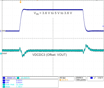
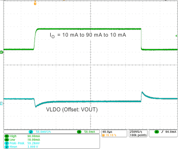
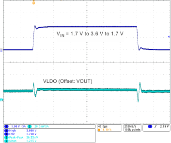
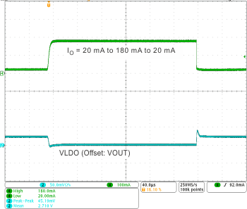
8.2.1.3 Application Curves
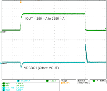
| VIN = 3.6 V | VO = 1.1375 V | ||
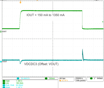
| VIN = 3.6 V | VO = 1.1375 V | ||
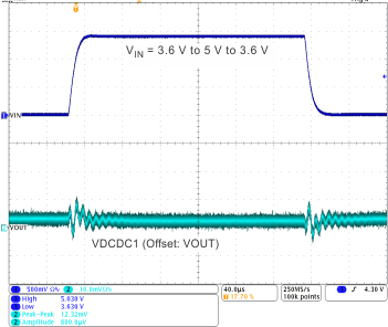
| VO = 1.1375 V | IO = 2500 mA | ||
| VO = 1.1375 V | IO = 1500 mA | ||
| VIN = 3.3 V | VO = 3.0 V | ||
| IO = 100 mA | VO = 1.2 V | ||
| VIN = 3.2 V | VO = 2.7 V | ||
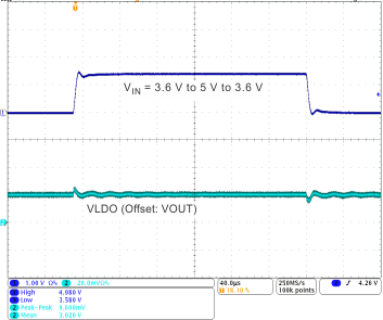
| IO = 100 mA | VO = 3.0 V | ||
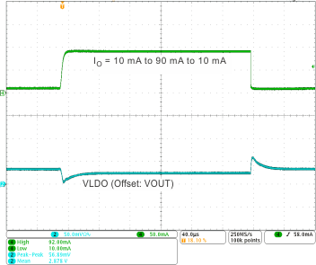
| VIN = 3.3 V | VO = 2.85 V | ||
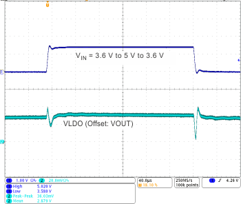
| IO = 100 mA | VO = 2.85 V | ||
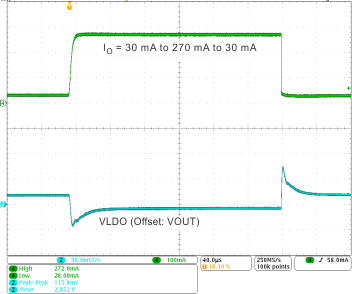
| VIN = 3.3 V | VO = 2.85 V | ||
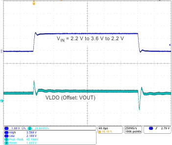
| IO = 300 mA | VO = 1.8 V | ||
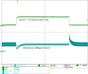
| VIN = 3.6 V | VO = 2.25 V | ||
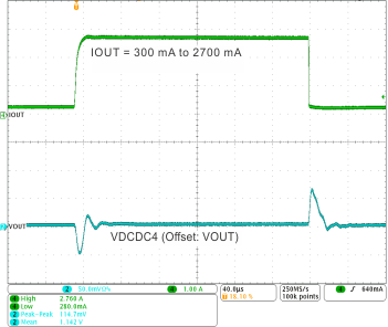
| VIN = 3.6 V | VO = 1.1375 V | ||
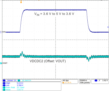
| VO = 1.8 V | IO = 750 mA | ||
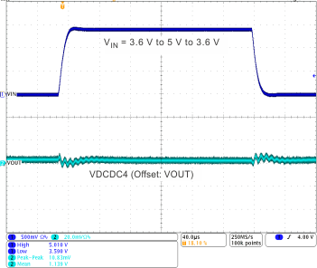
| VO = 1.1375 V | IO = 3000 mA | ||
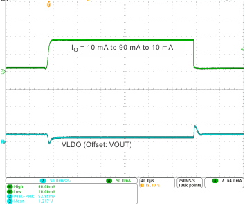
| VIN = 1.8 V | VO = 1.2 V | ||
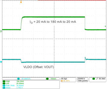
| VIN = 2.0 V | VO = 1.7 V | ||
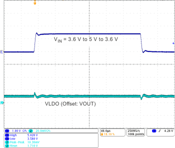
| IO = 100 mA | VO = 1.7 V | ||
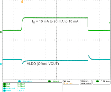
| VIN = 3.3 V | VO = 1.8 V | ||
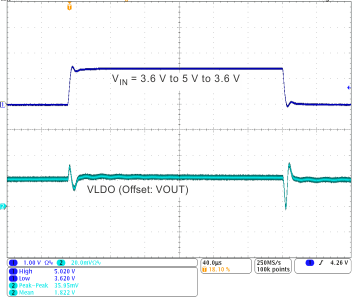
| IO = 100 mA | VO = 1.8 V | ||
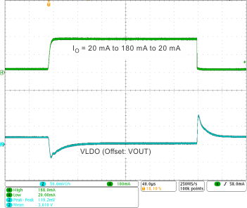
| VIN = 3.2 V | VO = 3.0 V | ||
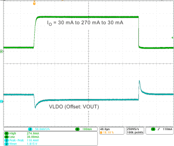
| VIN = 3.3 V | VO = 1.8 V | ||
8.2.1.4 Layout
8.2.1.4.1 Layout Guidelines
As for all switching power supplies, the layout is an important step in the design. Proper function of the device demands careful attention to PCB layout. Care must be taken in board layout to get the specified performance. If the layout is not carefully done, the regulators may show poor line and/or load regulation and stability issues, as well as EMI problems. It is critical to provide a low-impedance ground path. Therefore, use wide and short traces for the main current paths. The input capacitors must be placed as close as possible to the IC pins as well as the inductor and output capacitor.
Keep the common path to the GND pins, which returns the small signal components, and the high current of the output capacitors as short as possible to avoid ground noise. The VDCDCx trace should be connected right to the output capacitor and routed away from noisy components and traces (for example, the L1, L2, L3, and L4 traces).
The most critical connections are:
- PGNDx
- VDCDCx (positive output voltage sense connection)
- VDCDCx_GND (ground-sense connection)
- AGND
- VINDCDCx, VINDCDC_ANA, VCC
The PGNDx pins are the ground connections of the power stages, so they will carry high dc- and ac- peak currents. A low impedance connection to the GND-plane is needed, which must be independent from other pins in order not to couple noise into other pins. No other pins must be connected to PGNDx pins.
The VDCDCx pins are the positive-sense connections for the feedback loop. The connection must be made directly to the positive terminal of the pad of the output capacitor. Do not tie the pin to the pad of the output inductor or anywhere in between inductor and capacitor. It is also a good practice to shield the connection by GND traces or a GND-plane.
VDCDCx_GND is a sense connection for GND and is only available for DCDC1 and DCDC4. The connection can either be made to the GND pad of the output capacitor (preferred) or to the GND-plane directly if there is a solid connection of the GND-plane to the output capacitor. The pin must not be connected to the PGNDx pins as this will couple switching noise into the feedback loop.
The AGND (analog ground) pin is the main GND connection for internal analog circuitry. A proper connection must be made to a GND plane directly by a via. AGND and DGND (located next to each other) may be connected and a via each be used to the GND-plane.
VINDCDCx, VINDCD_ANA and VCC are supply-voltage-input terminals and need to be properly bypassed by their input capacitors. The CAPACITANCE needed is given in the Section 5.3. As ceramic capacitors will change their capacitance based on the voltage applied, temperature and age, the influence of these parameters need to be considered when choosing the value of a capacitor. The input capacitors are ideally placed on the same layer as the IC, so the connection can be made short and directly on the same layer with multiple vias used from the GND terminal to the GND-plane.
For details about the layout for TPS659121 and TPS659122, see the EVM user's guide, which can be found in the product folder on ti.com.
8.2.1.4.2 Layout Example
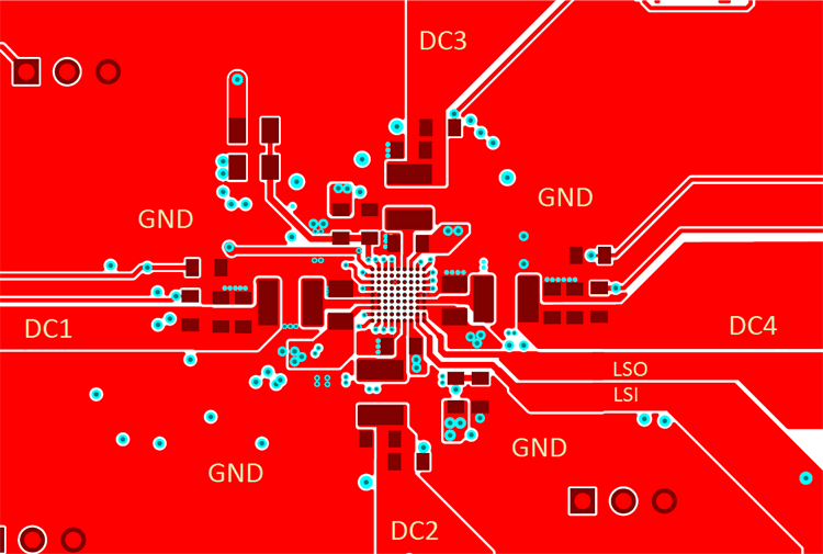 Figure 8-25 Layout Example
8.3 Power Supply Recommendations
The TPS65912 device is designed to work with an analog supply voltage range from 2.7 V to 5.5 V. The input supply should be well regulated and connected to the VCC pin, as well as the DCDC and LDO input pins. If the input supply is located more than a few inches from the TPS65912 device, additional capacitance may be required in addition to the recommended input capacitors at the VCC pin and the DCDC and LDO input pins.