SGLS118D December 2001 – September 2016
PRODUCTION DATA.
- 1 Features
- 2 Applications
- 3 Description
- 4 Revision History
- 5 Description (continued)
- 6 Pin Configuration and Functions
- 7 Specifications
- 8 Detailed Description
- 9 Application and Implementation
- 10Power Supply Recommendations
- 11Layout
- 12Device and Documentation Support
- 13Mechanical, Packaging, and Orderable Information
Package Options
Refer to the PDF data sheet for device specific package drawings
Mechanical Data (Package|Pins)
- DBV|5
Thermal pad, mechanical data (Package|Pins)
Orderable Information
11 Layout
11.1 Layout Guidelines
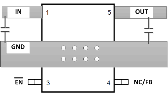
For the LDO power supply, especially these high voltage and large current ones, layout is an important step. If layout is not carefully designed, the regulator could not deliver enough output current because of the thermal limitation. To improve the thermal performance of the device, and maximize the current output at high ambient temperature, it is recommended to spread the GND as large as possible and put enough thermal vias on the thermal pad. Figure 27 shows an example layout.
11.2 Layout Example
 Figure 27. Layout Recommendation
11.3 Power Dissipation and Junction Temperature
Specified regulator operation is assured to a junction temperature of 125°C; the maximum junction temperature must be restricted to 125°C under normal operating conditions. This restriction limits the power dissipation the regulator can handle in any given application. To ensure the junction temperature is within acceptable limits, calculate the maximum allowable dissipation, PD(max), and the actual dissipation, PD, which must be less than or equal to PD(max).
The maximum-power-dissipation limit is determined using Equation 3.

where
- TJmax is the maximum allowable junction temperature
- RθJA is the thermal resistance junction-to-ambient for the package, see the dissipation rating table.
- TA is the ambient temperature.
The regulator dissipation is calculated using Equation 4.

Power dissipation resulting from quiescent current is negligible. Excessive power dissipation triggers the thermal protection circuit.