SGLS118D December 2001 – September 2016
PRODUCTION DATA.
- 1 Features
- 2 Applications
- 3 Description
- 4 Revision History
- 5 Description (continued)
- 6 Pin Configuration and Functions
- 7 Specifications
- 8 Detailed Description
- 9 Application and Implementation
- 10Power Supply Recommendations
- 11Layout
- 12Device and Documentation Support
- 13Mechanical, Packaging, and Orderable Information
Package Options
Refer to the PDF data sheet for device specific package drawings
Mechanical Data (Package|Pins)
- DBV|5
Thermal pad, mechanical data (Package|Pins)
Orderable Information
7 Specifications
7.1 Absolute Maximum Ratings
over operating free-air temperature range (unless otherwise noted)(1)| MIN | MAX | UNIT | ||
|---|---|---|---|---|
| Input voltage(2) | –0.3 | 13.5 | V | |
| Voltage range at EN | –0.3 | VI + 0.3 | V | |
| Voltage on OUT, FB | 7 | V | ||
| Peak output current | Internally Limited | |||
| Continuous total power dissipation | See Dissipation Ratings | |||
| TJ | Operating virtual junction temperature | –40 | 150 | °C |
| Tstg | Storage temperature | –65 | 150 | °C |
(1) Stresses beyond those listed under Absolute Maximum Ratings may cause permanent damage to the device. These are stress ratings only, and functional operation of the device at these or any other conditions beyond those indicated under Recommended Operating Conditions is not implied. Exposure to absolute-maximum-rated conditions for extended periods may affect device reliability.
(2) All voltage values are with respect to network ground terminal.
7.2 ESD Ratings
| VALUE | UNIT | |||
|---|---|---|---|---|
| V(ESD) | Electrostatic discharge | Human-body model (HBM), per ANSI/ESDA/JEDEC JS-001(1) | ±2000 | V |
| Charged-device model (CDM), per JEDEC specification JESD22-C101(2) | ±YYY | |||
(1) JEDEC document JEP155 states that 500-V HBM allows safe manufacturing with a standard ESD control process.
(2) JEDEC document JEP157 states that 250-V CDM allows safe manufacturing with a standard ESD control process.
7.3 Recommended Operating Conditions
over operating free-air temperature range (unless otherwise noted)| MIN | MAX | UNIT | ||
|---|---|---|---|---|
| VI | Input voltage(1) | 2.7 | 10 | V |
| VO | Output voltage | 1.2 | 5.5 | V |
| IO | Continuous output current(2) | 0 | 100 | mA |
| TJ | Operating junction temperature | —40 | 125 | °C |
(1) To calculate the minimum input voltage for your maximum output current, use the following formula: VI(min) = VO(max) + VDO(max load)
(2) Continuous output current and operating junction temperature are limited by internal protection circuitry, but it is not recommended that the device operate under conditions beyond those specified in this table for extended periods of time.
7.4 Thermal Information
| THERMAL METRIC(1) | TPS769xx-Q1 | UNIT | |
|---|---|---|---|
| DBV (SOT-23) | |||
| 5 PINS | |||
| RθJA | Junction-to-ambient thermal resistance | 204.6 | °C/W |
| RθJC(top) | Junction-to-case (top) thermal resistance | 117.5 | °C/W |
| RθJB | Junction-to-board thermal resistance | 34.4 | °C/W |
| ψJT | Junction-to-top characterization parameter | 11.8 | °C/W |
| ψJB | Junction-to-board characterization parameter | 33.5 | °C/W |
| RθJC(bot) | Junction-to-case (bottom) thermal resistance | — | °C/W |
(1) For more information about traditional and new thermal metrics, see the Semiconductor and IC Package Thermal Metrics application report.
7.5 Electrical Characteristics
over recommended operating free-air temperature range, VI = VO (typ) + 1 V, IO = 100 mA, EN = 0 V, Co = 4.7 µF (unless otherwise noted)| PARAMETER | TEST CONDITIONS | MIN | TYP | MAX | UNIT | |
|---|---|---|---|---|---|---|
| Output voltage (10 ∝A to 100 mA load)(1) |
TPS76901-Q1 | 1.2 V ≤ VO ≤ 5.5 V, TJ = 25°C | VO | V | ||
| 1.2 V ≤ VO ≤ 5.5 V, TJ = –40°C to 125°C | 0.97 VO | 1.03 VO | ||||
| TPS76912-Q1 | TJ = 25°C, 2.7 V < VIN < 10 V | 1.224 | ||||
| TJ = –40°C to 125°C, 2.7 V < VIN < 10 V | 1.187 | 1.261 | ||||
| TPS76915-Q1 | TJ = 25°C, 2.7 V < VIN < 10 V | 1.5 | ||||
| TJ = –40°C to 125°C, 2.7 V < VIN < 10 V | 1.455 | 1.545 | ||||
| TPS76918-Q1 | TJ = 25°C, 2.8 V < VIN < 10 V | 1.8 | ||||
| TJ = –40°C to 125°C, 2.8 V < VIN < 10 V | 1.746 | 1.854 | ||||
| TPS76925-Q1 | TJ = 25°C, 3.5 V < VIN < 10 V | 2.5 | ||||
| TJ = –40°C to 125°C, 3.5 V < VIN < 10 V | 2.425 | 2.575 | ||||
| TPS76927-Q1 | TJ = 25°C, 3.7 V < VIN < 10 V | 2.7 | ||||
| TJ = –40°C to 125°C, 3.7 V < VIN < 10 V | 2.619 | 2.781 | ||||
| TPS76928-Q1 | TJ = 25°C, 3.8 V < VIN < 10 V | 2.8 | ||||
| TJ = –40°C to 125°C, 3.8 V < VIN < 10 V | 2.716 | 2.884 | ||||
| TPS76930-Q1 | TJ = 25°C, 4 V < VIN < 10 V | 3 | ||||
| TJ = –40°C to 125°C, 4 V < VIN < 10 V | 2.91 | 3.09 | ||||
| TPS76933-Q1 | TJ = 25°C, 4.3 V < VIN < 10 V | 3.3 | ||||
| TJ = –40°C to 125°C, 4.3 V < VIN < 10 V | 3.201 | 3.399 | ||||
| TPS76950-Q1 | TJ = 25°C, 6 V < VIN < 10 V | 5 | ||||
| TJ = —40°C to 125°C, 6 V < VIN < 10 V | 4.85 | 5.15 | ||||
| Quiescent current (GND current)(1)(2) |
EN = 0 V, 0 mA < IO < 100 mA, TJ = 25°C | 17 | µA | |||
| EN = 0 V, IO = 100 mA, TJ = –40°C to 125°C | 28 | |||||
| Load regulation | EN = 0 V, IO = 0 to 100 mA, TJ = 25°C | 12 | mV | |||
| Output voltage line regulation (∆VO/VO) (2) |
VO + 1 V < VI ≤ 10 V, TJ = 25°C(1) | 0.04 | %/V | |||
| VO + 1 V < VI ≤ 10 V, TJ = –40°C to 125°C(1) | 0.1 | |||||
| Output noise voltage | BW = 300 Hz to 50 kHz, Co = 10 ∝F, TJ = 25°C | 190 | µVrms | |||
| Output current limit | VO = 0 V(1) | 350 | 750 | mA | ||
| Standby current | EN = VI, 2.7 < VI < 10 V | 1 | µA | |||
| TJ = —40°C to 125°C | 2 | |||||
| FB input current | FB = 1.224 V (TPS76901-Q1) | –1 | 1 | µA | ||
| High level enable input voltage | 2.7 V < VI < 10 V | 1.7 | V | |||
| Low level enable input voltage | 2.7 V < VI < 10 V | 0.9 | V | |||
| Power supply ripple rejection | f = 1 kHz, Co = 10 ∝F, TJ = 25°C | 60 | dB | |||
| Input current (EN) | EN = 0 V | –1 | 0 | 1 | µA | |
| EN = VI | –1 | 1 | ||||
| Dropout voltage(3) | TPS76928-Q1 | IO = 50 mA, TJ = 25°C | 60 | mV | ||
| IO = 50 mA, TJ = –40°C to 125°C | 125 | |||||
| IO = 100 mA, TJ = 25°C | 122 | |||||
| IO = 100 mA, TJ = –40°C to 125°C | 245 | |||||
| TPS76930-Q1 | IO = 50 mA, TJ = 25°C | 57 | ||||
| IO = 50 mA, TJ = –40°C to 125°C | 115 | |||||
| IO = 100 mA, TJ = 25°C | 115 | |||||
| IO = 100 mA, TJ = –40°C to 125°C | 230 | |||||
| TPS76933-Q1 | IO = 50 mA, TJ = 25°C | 48 | ||||
| IO = 50 mA, TJ = –40°C to 125°C | 100 | |||||
| IO = 100 mA, TJ = 25°C | 98 | |||||
| IO = 100 mA, TJ = –40°C to 125°C | 200 | |||||
| TPS76950-Q1 | IO = 50 mA, TJ = 25°C | 35 | ||||
| IO = 50 mA, TJ = –40°C to 125°C | 85 | |||||
| IO = 100 mA, TJ = 25°C | 71 | |||||
| IO = 100 mA, TJ = –40°C to 125°C | 170 | |||||
(1) Minimum IN operating voltage is 2.7 V or VO (typ) + 1 V, whichever is greater. The maximum IN voltage is 10 V, minimum output current is 10 µA, and maximum output current is 100 mA.
(2) If VO ≤ 1.8 V then VImin = 2.7 V, VImax = 10 V:

If VO ≥ 2.5 V then VImin = VO + 1 V, VImax = 10 V:


If VO ≥ 2.5 V then VImin = VO + 1 V, VImax = 10 V:

(3) The IN voltage equals VO (typ) — 100 mV; the TPS76901-Q1 output voltage is set to 3.3 V nominal with an external resistor divider. TPS76912-Q1, TPS76915-Q1, TPS76918-Q1, TPS76925-Q1, and TPS76927-Q1 dropout voltage is limited by input voltage range limitations.
7.6 Dissipation Ratings
| BOARD | PACKAGE | RθJC | RθJA | DERATING FACTOR ABOVE TA = 25°C |
TA ≤ 25°C POWER RATING |
TA = 70°C POWER RATING |
TA = 85°C POWER RATING |
|---|---|---|---|---|---|---|---|
| Low K(1) | DBV | 65.8°C/W | 259°C/W | 3.9 mW/°C | 386 mW | 212 mW | 154 mW |
| High K(2) | DBV | 65.8°C/W | 180°C/W | 5.6 mW/°C | 555 mW | 305 mW | 222 mW |
(1) The JEDEC Low K (1s) board design used to derive this data was a 3 inch x 3 inch, two layer board with 2 ounce copper traces on top of the board.
(2) The JEDEC High K (2s2p) board design used to derive this data was a 3 inch x 3 inch, multilayer board with 1 ounce internal power and ground planes and 2 ounce copper traces on top and bottom of the board.
7.7 Typical Characteristics
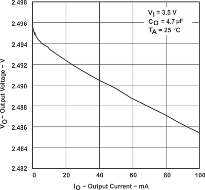 Figure 1. TPS76925-Q1 Output Voltage vs Output Current
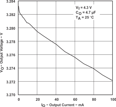 Figure 3. TPS76933-Q1 Output Voltage vs Output Current
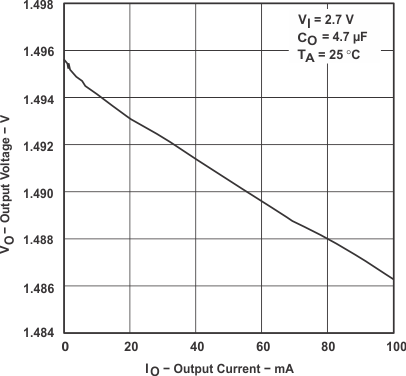 Figure 2. TPS76915-Q1 Output Voltage vs Output Current
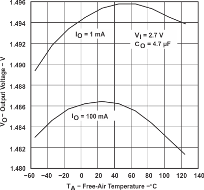 Figure 4. TPS76915-Q1 Output Voltage vs Free-Air Temperature
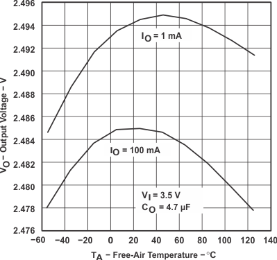 Figure 5. TPS76925-Q1 Output Voltage vs Free-Air Temperature
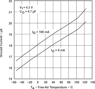 Figure 7. TPS76933-Q1 Ground Current vs Free-Air Temperature
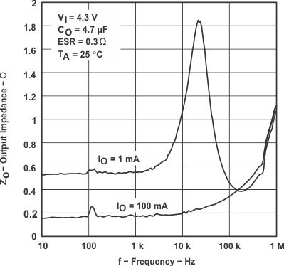 Figure 9. Output Impedance vs Frequency
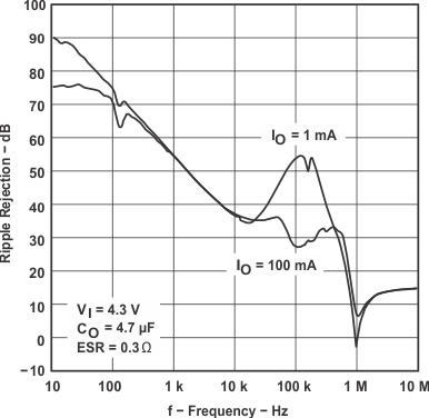 Figure 11. TPS76933-Q1 Ripple Rejection vs Frequency
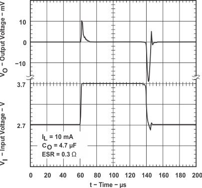 Figure 13. TPS76915-Q1 Line Transient Response
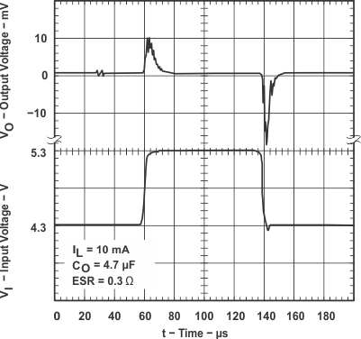 Figure 15. TPS76933-Q1 Line Transient Response
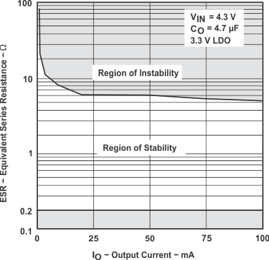 Figure 17. TPS76933-Q1 Typical Regions of Stability Equivalent Series Resistance (ESR) vs Output Current
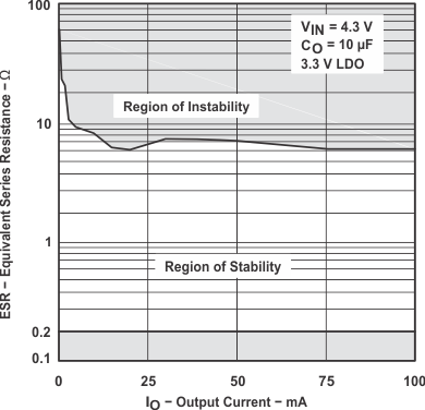 Figure 19. TPS76933-Q1 Typical Regions of Stability Equivalent Series Resistance (ESR) vs Output Current
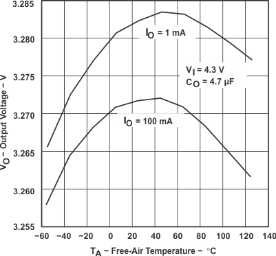 Figure 6. TPS76933-Q1 Output Voltage vs Free-Air Temperature
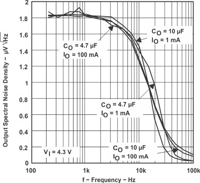 Figure 8. TPS76933-Q1 Output Spectral Noise Density vs Frequency
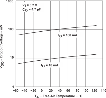 Figure 10. TPS76933-Q1 Dropout Voltage vs Free-Air Temperature
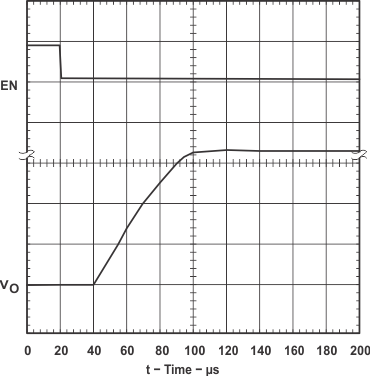 Figure 12. LDO Start-Up Time
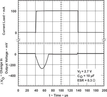 Figure 14. TPS76915-Q1 Load Transient Response
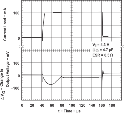 Figure 16. TPS76933-Q1 Load Transient Response
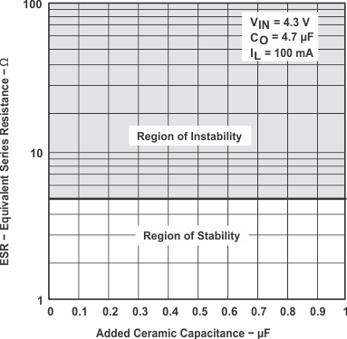 Figure 18. TPS76933-Q1 Typical Regions of Stability Equivalent Series Resistance (ESR) vs Added Ceramic Capacitance
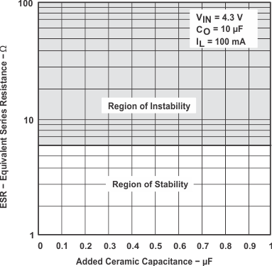 Figure 20. TPS76933-Q1 Typical Regions of Stability Equivalent Series Resistance (ESR) vs Added Ceramic Capacitance