SBVS133A February 2010 – November 2014 TPS783
PRODUCTION DATA.
- 1 Features
- 2 Applications
- 3 Description
- 4 Revision History
- 5 Pin Configuration and Functions
- 6 Specifications
- 7 Detailed Description
- 8 Application and Implementation
- 9 Power-Supply Recommendations
- 10Layout
- 11Device and Documentation Support
- 12Mechanical, Packaging, and Orderable Information
Package Options
Mechanical Data (Package|Pins)
- DDC|5
Thermal pad, mechanical data (Package|Pins)
Orderable Information
10 Layout
10.1 Layout Guidelines
10.1.1 Board Layout Recommendations to Improve PSRR and Noise Performance
To improve ac performance (such as PSRR, output noise, and transient response), design the printed circuit board (PCB) with separate ground planes for VIN and VOUT, with each ground plane connected only at the GND pin of the device. In addition, the output capacitor must be as close as possible to the ground pin of the device to provide a common reference for regulation purposes. High ESR capacitors may degrade PSRR.
10.1.2 Package Mounting
Solder pad footprint recommendations for the TPS783 series are available from the Texas Instruments website at www.ti.com through the TPS783 family product folders.
10.1.3 Thermal Information
10.1.3.1 Thermal Protection
Thermal protection disables the device output when the junction temperature rises to approximately 160°C, allowing the device to cool. After the junction temperature cools to approximately 140°C, the output circuitry is enabled. Depending on power dissipation, thermal resistance, and ambient temperature, the thermal protection circuit may cycle on and off again. This cycling limits the dissipation of the regulator, protecting it from damage as a result of overheating.
Any tendency to activate the thermal protection circuit indicates excessive power dissipation or an inadequate heatsink. For reliable operation, limit junction temperature to 105°C maximum. To estimate the margin of safety in a complete design (including heatsink), increase the ambient temperature until the thermal protection is triggered; use worst-case loads and signal conditions.
The internal protection circuitry of the TPS783 family is designed to protect against overload conditions. However, this circuitry is not intended to replace proper heatsinking. Continuously running the TPS783 series into thermal shutdown degrades device reliability.
10.1.3.2 Power Dissipation
The ability to remove heat from the die is different for each package type, presenting different considerations in the PCB layout. The PCB area around the device that is free of other components moves the heat from the device to the ambient air. Performance data for JEDEC low- and high-K boards are given in the Thermal Information table. Using heavier copper increases the effectiveness in removing heat from the device. The addition of plated through-holes to heat-dissipating layers also improves the heatsink effectiveness. Power dissipation depends on input voltage and load conditions. Power dissipation (PD) is equal to the product of the output current times the voltage drop across the output pass element (VIN to VOUT), as shown in Equation 2:

10.2 Layout Example
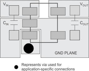 Figure 25. TPS783xx Layout Example