SLVSAA0E November 2010 – March 2020 TPS7A6201-Q1
PRODUCTION DATA.
- 1 Features
- 2 Applications
- 3 Description
- 4 Revision History
- 5 Pin Configuration and Functions
- 6 Specifications
- 7 Detailed Description
- 8 Application and Implementation
- 9 Power Supply Recommendations
- 10Layout
- 11Device and Documentation Support
- 12Mechanical, Packaging, and Orderable Information
Package Options
Refer to the PDF data sheet for device specific package drawings
Mechanical Data (Package|Pins)
- KTT|5
Thermal pad, mechanical data (Package|Pins)
- KTT|5
Orderable Information
5 Pin Configuration and Functions
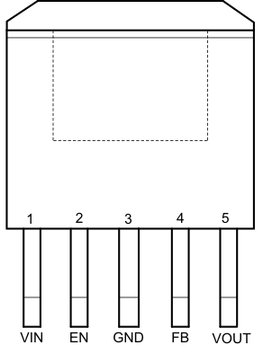
KTT Package
5-Pin TO-263
Top View

Pin Functions
| PIN | I/O | DESCRIPTION | |
|---|---|---|---|
| NO. | NAME | ||
| 1 | VIN | I | Input voltage pin: The unregulated input voltage is supplied to this pin. A bypass capacitor shall be connected between VIN pin and GND pin to dampen input line transients. |
| 2 | EN | I | Enable pin: This is a high voltage tolerant input pin with an internal pulldown. A high input to this pin activates the device and turns the regulator ON. This input can be connected to VIN terminal for self bias applications. If this pin is not connected, the device stays disabled. |
| 3 | GND | I/O | Ground pin: This is signal ground pin of the IC. |
| 4 | FB | I | Feedback pin: This pin is used to connect external resistors to ground to program the output voltage. |
| 5 | VOUT | O | Regulated output voltage pin: This is a regulated output voltage pin with a limitation on maximum output current. An external resistor divider is connected at this pin to program the output voltage. To achieve stable operation and prevent oscillation, an external output capacitor (COUT) with low ESR shall be connected between this pin and GND pin. |