SLVSDW6C April   2017  – April 2021 TPS7H1101A-SP

PRODUCTION DATA  

  1. Features
  2. Applications
  3. Description
  4. Revision History
  5. Pin Configuration and Functions
  6. Specifications
    1. 6.1 Absolute Maximum Ratings
    2. 6.2 ESD Ratings
    3. 6.3 Recommended Operating Conditions
    4. 6.4 Thermal Information
    5. 6.5 Electrical Characteristics
    6. 6.6 Typical Characteristics
  7. Detailed Description
    1. 7.1 Overview
    2. 7.2 Functional Block Diagram
    3. 7.3 Feature Description
      1. 7.3.1 Soft Start
      2. 7.3.2 Power Good (PG)
    4. 7.4 Device Functional Modes
      1. 7.4.1 Enable/Disable
  8. Application and Implementation
    1. 8.1 Application Information
      1. 8.1.1 Stability
    2. 8.2 Typical Application
      1. 8.2.1 Detailed Design Procedure
        1. 8.2.1.1 Adjustable Output Voltage (Feedback Circuit)
        2. 8.2.1.2 PCL
        3. 8.2.1.3 High-Side Current Sense
        4. 8.2.1.4 Current Foldback
        5. 8.2.1.5 Transient Response
        6. 8.2.1.6 Current Sharing
        7. 8.2.1.7 Compensation
        8. 8.2.1.8 Output Noise
        9. 8.2.1.9 Capacitors
      2. 8.2.2 Application Curves
  9. Power Supply Recommendations
  10. 10Layout
    1. 10.1 Layout Guidelines
    2. 10.2 Layout Example
  11. 11Device and Documentation Support
    1. 11.1 Device Support
      1. 11.1.1 Third-Party Products Disclaimer
      2. 11.1.2 Device Nomenclature
    2. 11.2 Documentation Support
      1. 11.2.1 Related Documentation
    3. 11.3 Receiving Notification of Documentation Updates
    4. 11.4 Support Resources
    5. 11.5 Trademarks
    6. 11.6 Electrostatic Discharge Caution
    7. 11.7 Glossary
  12. 12Mechanical, Packaging, and Orderable Information

Package Options

Mechanical Data (Package|Pins)
Thermal pad, mechanical data (Package|Pins)
Orderable Information

Description

The TPS7H1101A-SP is an improved version of the TPS7H1101-SP allowing the use of the enable feature across the entire input voltage range. It is a radiation-hardened LDO linear regulator that uses a PMOS pass element configuration. It operates over a wide range of input voltage, from 1.5 V to 7 V while offering excellent PSRR. The TPS7H1101A-SP features a precise and programmable foldback current limit implementation with a very-wide adjustment range. To support the complex power requirements of FPGAs, DSPs, or microcontrollers, the TPS7H1101A-SP provides enable on and off functionality, programmable soft start, current sharing capability, and a Power Good open-drain output.

Device Information
PART NUMBER(1)GRADEPACKAGE
5962R1320202V9AKGD Flight Grade RHA 100 krad(Si)16-Pin CFP
9.60 mm × 11.00 mm
Weight: 1.55 g(4)
5962R1320202VXCFlight Grade RHA 100 krad(Si)
TPS7H1101HKR/EMEngineering Modules(3)(5)
TPS7H1101AHKR/EM Engineering Modules(3)
TPS7H1101SPEVMCeramic Evaluation BoardEVM
For all available packages, see the orderable addendum at the end of the data sheet.
See Radiation Report (SNAA257) for details.
These units are intended for engineering evaluation only. They are processed to a noncompliant flow (that is, no burn-in, and so forth) and are tested to a temperature rating of 25°C only. These units are not suitable for qualification, production, radiation testing or flight use. Parts are not warranted for performance over the full MIL specified temperature range of –55°C to 125°C or operating life.
Weight is accurate to ±10%.
TPS7H1101HKR/EM with device Date Code newer than 1705 is equivalent to TPS7H1101AHKR/EM using rev A silicon.
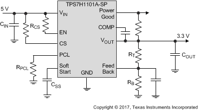
GUID-4853443B-76DA-4AFA-AD00-6C48C967BC63-low.gifTypical Application Circuit