SLUSCZ1 May   2017 TPS92518-Q1

PRODUCTION DATA.  

  1. Features
  2. Applications
  3. Description
    1.     Device Images
      1.      Simplified Schematic
  4. Revision History
  5. Pin Configuration and Functions
    1.     Pin Functions
  6. Specifications
    1. 6.1 Absolute Maximum Ratings
    2. 6.2 ESD Ratings
    3. 6.3 Recommended Operating Conditions
    4. 6.4 Thermal Information
    5. 6.5 Electrical Characteristics
    6. 6.6 Typical Characteristics
  7. Parameter Measurement Information
    1. 7.1 CSN Pin Falling Delay (tDEL)
    2. 7.2 Off-Timer (tOFF)
  8. Detailed Description
    1. 8.1 Overview
    2. 8.2 Functional Block Diagram
    3. 8.3 Feature Description
      1. 8.3.1  General Operation
        1. 8.3.1.1 Constant Off-Time vs. Constant µs×V operation
        2. 8.3.1.2 Output Equation
        3. 8.3.1.3 OFF Timer
          1. 8.3.1.3.1 Off-time and Maximum Off-time Calculations
      2. 8.3.2  Important System Considerations: Off-Timer and Maximum Peak Threshold Values
        1. 8.3.2.1 Peak Current Sense Comparator
        2. 8.3.2.2 Peak Current Threshold - LEDx _PKTH_DAC
        3. 8.3.2.3 Off-Time Thresholds - LEDx_TOFF_DAC and LEDx_MAXOFF_DAC
      3. 8.3.3  Shunt FET or Matrix dimming: Maximum Off-timer Calculation
        1. 8.3.3.1 Output Ringing and TPS92518-Q1 Protection
        2. 8.3.3.2 Live Peak and Off-Time Threshold Changes
      4. 8.3.4  VIN and the VCC Internal Regulators
      5. 8.3.5  Output Enable Control Logic
        1. 8.3.5.1 EN/UV2 - SPI Control Bypass
      6. 8.3.6  BOOT Capacitor and BOOT UVLO
      7. 8.3.7  Drop-out Operation
        1. 8.3.7.1 Early Drop-Out (Boot Capacitor Voltage >> VBOOT-UVLO)
        2. 8.3.7.2 Full Drop-Out (Boot Capacitor Voltage reaching VBOOT-UVLO)
        3. 8.3.7.3 Minimum BOOT Voltage and FET Control
        4. 8.3.7.4 BOOT Controlled internal Pull-Down
      8. 8.3.8  Analog and PWM Dimming
        1. 8.3.8.1 Dimming Methods
        2. 8.3.8.2 PWMx Pin Operation
        3. 8.3.8.3 PWM Dimming - Current Rise Performance
        4. 8.3.8.4 PWM and Analog Dimming - Linearity Limitations and Buck Converters
          1. 8.3.8.4.1 PWM:
          2. 8.3.8.4.2 ANALOG:
        5. 8.3.8.5 DCM Current Calculation
        6. 8.3.8.6 Current Sharing
      9. 8.3.9  VIN and CSPx Pin Configuration
      10. 8.3.10 Enable and Undervoltage Lock-out Configuration
      11. 8.3.11 Voltage Sampling and DAC Operation
        1. 8.3.11.1 ADC Control and LED Voltage Updating
      12. 8.3.12 Device Functional Modes
        1. 8.3.12.1 Analog Dimming
        2. 8.3.12.2 PWM Dimming
    4. 8.4 Serial Interface
      1. 8.4.1 Command Frame
      2. 8.4.2 Response Frame Formats
        1. 8.4.2.1 Read Response Frame Format
        2. 8.4.2.2 Write Response Frame Format
        3. 8.4.2.3 Write Error/POR Frame Format
        4. 8.4.2.4 SPI Error
    5. 8.5 Registers
      1. 8.5.1  CONTROL Register (Address = 00h) [reset = 00h]
        1. Table 3. CONTROL Register Field Descriptions
      2. 8.5.2  STATUS (FAULT) Register (Address = 01h) [reset = 10h]
        1. Table 4. STATUS Register Field Descriptions
      3. 8.5.3  THERM_WARN_LMT Register (Address = 02h) [reset = 80h]
        1. Table 5. THERM_WARN_LMT Register Field Descriptions
      4. 8.5.4  LED1_PKTH_DAC Register (Address = 03h) [reset = 80h]
        1. Table 6. LED1_PKTH_DAC Register Field Descriptions
      5. 8.5.5  LED2_PKTH_DAC Register (Address = 04h) [reset = 80h]
        1. Table 7. LED2_PKTH_DAC Register Field Descriptions
      6. 8.5.6  LED1_TOFF_DAC Register (Address = 05h) [reset = 80h]
        1. Table 8. LED1_TOFF_DAC Register Field Descriptions
      7. 8.5.7  LED2_TOFF_DAC Register (Address = 06h) [reset = 80h]
        1. Table 9. LED2_TOFF_DAC Register Field Descriptions
      8. 8.5.8  LED1_MAXOFF_DAC Register (Address = 07h) [reset = 80h]
        1. Table 10. LED1_MAXOFF_DAC Register Field Descriptions
      9. 8.5.9  LED2_MAXOFF_DAC Register (Address = 08h) [reset = 80h]
        1. Table 11. LED2_MAXOFF_DAC Register Field Descriptions
      10. 8.5.10 VTHERM Register (Address = 09h) [reset = 0h]
        1. Table 12. VTHERM Register Field Descriptions
      11. 8.5.11 LED1_MOST_RECENT Register (Address = 0Ah) [reset = 0h]
        1. Table 13. LED1_MOST_RECENT Register Field Descriptions
      12. 8.5.12 LED1_LAST_ON Register (Address = 0Bh) [reset = 0h]
        1. Table 14. LED1_LAST_ON Register Field Descriptions
      13. 8.5.13 LED1_LAST_OFF Register (Address = 0Ch) [reset = 0h]
        1. Table 15. LED1_LAST_OFF Register Field Descriptions
      14. 8.5.14 LED2_MOST_RECENT Register (Address = 0Dh) [reset = 0h]
        1. Table 16. LED2_MOST_RECENT Register Field Descriptions
      15. 8.5.15 LED2_LAST_ON Register (Address = 0Eh) [reset = 0h]
        1. Table 17. LED2_LAST_ON Register Field Descriptions
      16. 8.5.16 LED2_LAST_OFF Register (Address = 0Fh) [reset = 0h]
        1. Table 18. LED2_LAST_OFF Register Field Descriptions
      17. 8.5.17 Reset Register (Address = 10h) [reset = 0h]
        1. Table 19. Reset Register Field Descriptions
    6. 8.6 Programming
      1. 8.6.1 TPS92518-Q1 Register Typedef - Sample Code
      2. 8.6.2 Command Frame - Sample Code
      3. 8.6.3 SPI Read/Write - Sample Code
  9. Application and Implementation
    1. 9.1 Application Information
    2. 9.2 Typical Application
      1. 9.2.1 Design Requirements
      2. 9.2.2 Detailed Design Procedure
      3. 9.2.3 Application Curves
    3. 9.3 Dos and Don'ts
  10. 10Power Supply Recommendations
    1. 10.1 Input Source Direct from Battery
    2. 10.2 Input Source from a Boost Stage
  11. 11Layout
    1. 11.1 Layout Guidelines
    2. 11.2 Layout Example
  12. 12Device and Documentation Support
    1. 12.1 Receiving Notification of Documentation Updates
    2. 12.2 Community Resources
    3. 12.3 Trademarks
    4. 12.4 Electrostatic Discharge Caution
    5. 12.5 Glossary
  13. 13Mechanical, Packaging, and Orderable Information

Package Options

Mechanical Data (Package|Pins)
Thermal pad, mechanical data (Package|Pins)
Orderable Information

Early Drop-Out (Boot Capacitor Voltage >> VBOOT-UVLO)

the first effects of drop-out can be seen when the input voltage approaches a few volts above the output voltage. Unless there is sufficient output capacitance, the change in the LED voltage during the ramp up of the inductor and output current can cause a non-linearity in the ramp.
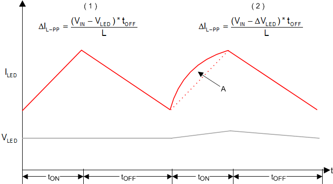
TPS92518-Q1 EarlyDropOut.gifFigure 24. Inductor on-time Current Non-linearity

In case (1) shown in , VIN-VLED is sufficiently large that variations in VLED are not relevant and/or not present because of sufficient output capacitance.

In case (2), VIN and VLED are closer in value making the difference lower and more easily affected by variations in VLED. ΔVLED is the total variation in the voltage across the inductor and includes the ILED x RL-DCR voltage drop which also changes with IL and impacts the inductor current linearity. The combination of factors leads to an inductor current on-time non-linearity which increases the average value of the inductor current, and hence the LED current. This means the first affect of approaching drop-out is always an increase in LED current.

It is important to note that the output current is always limited to the peak limit set by the internal programmed reference and the sense resistor. (The peak current threshold) This means a design having a smaller overall inductor current ripple (smaller ΔIL-PP) will have less error when a drop-out condition occurs.