SLVSC76E February   2014  – May 2018 TPS92630-Q1

PRODUCTION DATA.  

  1. Features
  2. Applications
  3. Description
  4. Typical Application Schematic
  5. Revision History
  6. Description (Continued)
  7. Pin Configuration and Functions
    1.     Pin Functions
  8. Specifications
    1. 8.1 Absolute Maximum Ratings
    2. 8.2 ESD Ratings
    3. 8.3 Recommended Operating Conditions
    4. 8.4 Thermal Information
    5. 8.5 Electrical Characteristics
    6. 8.6 Timing Requirements
    7. 8.7 Typical Characteristics
  9. Parameter Measurement Information
  10. 10Detailed Description
    1. 10.1 Overview
    2. 10.2 Functional Block Diagram
    3. 10.3 Feature Description
      1. 10.3.1 Constant LED-Current Setting
      2. 10.3.2 PWM Control
      3. 10.3.3 FAULT Diagnostics
      4. 10.3.4 Short-Circuit Detection
      5. 10.3.5 Open-Load Detection
      6. 10.3.6 Thermal Foldback
    4. 10.4 Device Functional Modes
      1. 10.4.1 Thermal Information
      2. 10.4.2 Operation With V(VIN) < 5 V (Minimum V(VIN))
      3. 10.4.3 Operation With 5 V < V(VIN) < 9 V (Lower-Than-Normal Automotive Battery Voltage)
  11. 11Applications and Implementation
    1. 11.1 Application Information
    2. 11.2 Typical Applications
      1. 11.2.1 Stoplight and Taillight Application With PWM Generator
        1. 11.2.1.1 Design Requirements
        2. 11.2.1.2 Detailed Design Procedure
          1. 11.2.1.2.1 Step-by-Step Design Procedure
            1. 11.2.1.2.1.1 R(REF)
            2. 11.2.1.2.1.2 Duty Cycle
            3. 11.2.1.2.1.3 Input and Output Capacitors
        3. 11.2.1.3 PWM Dimming Application Curve
      2. 11.2.2 Simple Stop-Light and Taillight Application
        1. 11.2.2.1 Design Requirements
        2. 11.2.2.2 Detailed Design Procedure
          1. 11.2.2.2.1 Step-by-Step Design Procedure
            1. 11.2.2.2.1.1 R(REF)
            2. 11.2.2.2.1.2 R(Stop)
            3. 11.2.2.2.1.3 Input and Output Capacitors
      3. 11.2.3 Parallel Connection
        1. 11.2.3.1 Design Requirements
        2. 11.2.3.2 Detailed Design Procedure
          1. 11.2.3.2.1 Step-by-Step Design Procedure
            1. 11.2.3.2.1.1 R(REF)
            2. 11.2.3.2.1.2 Input and Output Capacitors
      4. 11.2.4 Alternate Parallel Connection
        1. 11.2.4.1 Design Requirements
        2. 11.2.4.2 Detailed Design Procedure
          1. 11.2.4.2.1 Step-by-Step Design Procedure
            1. 11.2.4.2.1.1 R(REF)
            2. 11.2.4.2.1.2 Input and Output Capacitors
      5. 11.2.5 High-Side PWM Dimming
        1. 11.2.5.1 Design Requirements
        2. 11.2.5.2 Detailed Design Procedure
          1. 11.2.5.2.1 Step-by-Step Design Procedure
            1. 11.2.5.2.1.1 Ratio of Resistors, R1 / R2
            2. 11.2.5.2.1.2 R1 and R2 Selection
            3. 11.2.5.2.1.3 Input and Output Capacitors
  12. 12Power Supply Recommendations
  13. 13Layout
    1. 13.1 Layout Guidelines
    2. 13.2 Layout Example
  14. 14Device and Documentation Support
    1. 14.1 Documentation Support
      1. 14.1.1 Related Documentation
    2. 14.2 Receiving Notification of Documentation Updates
    3. 14.3 Community Resources
    4. 14.4 Trademarks
    5. 14.5 Electrostatic Discharge Caution
    6. 14.6 Glossary
  15. 15Mechanical, Packaging, and Orderable Information

Package Options

Mechanical Data (Package|Pins)
Thermal pad, mechanical data (Package|Pins)
Orderable Information

FAULT Diagnostics

The TPS92630-Q1 device has two fault pins, FAULT and FAULT_S. FAULT_S is a dedicated fault pin for single-LED short failure and FAULT is for general faults, that is, short, open, and thermal shutdown. The dual pins allow maximum flexibility based on all requirements and application conditions.

The device fault pins can be connected to an MCU for fault reporting. Both fault pins are open-drain transistors with a weak internal pullup. See Figure 19.

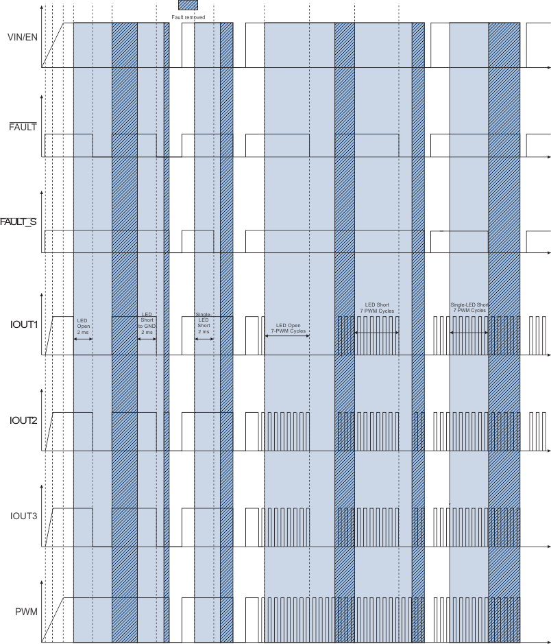
TPS92630-Q1 det_tim_dia_1_SLVSC76.gifFigure 18. Detailed Timing Diagram

In case there is no MCU, one can connect up to 15 TPS92630-Q1 FAULT and FAULT_S pins together. When one or more devices have errors, the respective FAULT̅ pins go low, pulling the connected FAULT bus down and shutting down all device outputs. Figure 19 shows the fault-line bus connection.
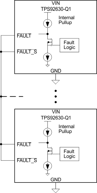
TPS92630-Q1 fau_lin_conn_SLVSC76.gifFigure 19. Fault-Line Bus Connection

The device releases the FAULT bus when external circuitry pulls the FAULT pin high, on toggling of the EN pin, or on a power cycle of the device. In case there is no MCU, only a power cycle clears the fault. See Figure 20.
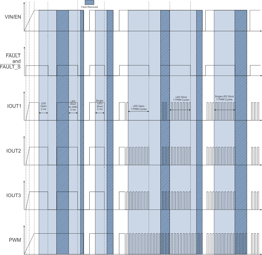
TPS92630-Q1 det_tim_dia_2_SLVSC76.gifFigure 20. Detailed Timing Diagram

The following faults result in the FAULT or FAULT_S pin going low: thermal shutdown, open load, output short circuit, single LED short, and REF open or shorted. For thermal shutdown or LED open, release of the FAULT pin occurs when the thermal-shutdown or LED-open condition no longer exists. For other faults, the FAULT and FAULT_S pins stay low even if the condition does not exist. Clearing the faults requires a power cycle of the device.