SLVSC76E February   2014  – May 2018 TPS92630-Q1

PRODUCTION DATA.  

  1. Features
  2. Applications
  3. Description
  4. Typical Application Schematic
  5. Revision History
  6. Description (Continued)
  7. Pin Configuration and Functions
    1.     Pin Functions
  8. Specifications
    1. 8.1 Absolute Maximum Ratings
    2. 8.2 ESD Ratings
    3. 8.3 Recommended Operating Conditions
    4. 8.4 Thermal Information
    5. 8.5 Electrical Characteristics
    6. 8.6 Timing Requirements
    7. 8.7 Typical Characteristics
  9. Parameter Measurement Information
  10. 10Detailed Description
    1. 10.1 Overview
    2. 10.2 Functional Block Diagram
    3. 10.3 Feature Description
      1. 10.3.1 Constant LED-Current Setting
      2. 10.3.2 PWM Control
      3. 10.3.3 FAULT Diagnostics
      4. 10.3.4 Short-Circuit Detection
      5. 10.3.5 Open-Load Detection
      6. 10.3.6 Thermal Foldback
    4. 10.4 Device Functional Modes
      1. 10.4.1 Thermal Information
      2. 10.4.2 Operation With V(VIN) < 5 V (Minimum V(VIN))
      3. 10.4.3 Operation With 5 V < V(VIN) < 9 V (Lower-Than-Normal Automotive Battery Voltage)
  11. 11Applications and Implementation
    1. 11.1 Application Information
    2. 11.2 Typical Applications
      1. 11.2.1 Stoplight and Taillight Application With PWM Generator
        1. 11.2.1.1 Design Requirements
        2. 11.2.1.2 Detailed Design Procedure
          1. 11.2.1.2.1 Step-by-Step Design Procedure
            1. 11.2.1.2.1.1 R(REF)
            2. 11.2.1.2.1.2 Duty Cycle
            3. 11.2.1.2.1.3 Input and Output Capacitors
        3. 11.2.1.3 PWM Dimming Application Curve
      2. 11.2.2 Simple Stop-Light and Taillight Application
        1. 11.2.2.1 Design Requirements
        2. 11.2.2.2 Detailed Design Procedure
          1. 11.2.2.2.1 Step-by-Step Design Procedure
            1. 11.2.2.2.1.1 R(REF)
            2. 11.2.2.2.1.2 R(Stop)
            3. 11.2.2.2.1.3 Input and Output Capacitors
      3. 11.2.3 Parallel Connection
        1. 11.2.3.1 Design Requirements
        2. 11.2.3.2 Detailed Design Procedure
          1. 11.2.3.2.1 Step-by-Step Design Procedure
            1. 11.2.3.2.1.1 R(REF)
            2. 11.2.3.2.1.2 Input and Output Capacitors
      4. 11.2.4 Alternate Parallel Connection
        1. 11.2.4.1 Design Requirements
        2. 11.2.4.2 Detailed Design Procedure
          1. 11.2.4.2.1 Step-by-Step Design Procedure
            1. 11.2.4.2.1.1 R(REF)
            2. 11.2.4.2.1.2 Input and Output Capacitors
      5. 11.2.5 High-Side PWM Dimming
        1. 11.2.5.1 Design Requirements
        2. 11.2.5.2 Detailed Design Procedure
          1. 11.2.5.2.1 Step-by-Step Design Procedure
            1. 11.2.5.2.1.1 Ratio of Resistors, R1 / R2
            2. 11.2.5.2.1.2 R1 and R2 Selection
            3. 11.2.5.2.1.3 Input and Output Capacitors
  12. 12Power Supply Recommendations
  13. 13Layout
    1. 13.1 Layout Guidelines
    2. 13.2 Layout Example
  14. 14Device and Documentation Support
    1. 14.1 Documentation Support
      1. 14.1.1 Related Documentation
    2. 14.2 Receiving Notification of Documentation Updates
    3. 14.3 Community Resources
    4. 14.4 Trademarks
    5. 14.5 Electrostatic Discharge Caution
    6. 14.6 Glossary
  15. 15Mechanical, Packaging, and Orderable Information

Package Options

Mechanical Data (Package|Pins)
Thermal pad, mechanical data (Package|Pins)
Orderable Information

Typical Characteristics

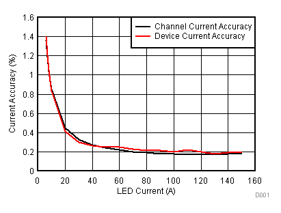
TPS92630-Q1 D001_SLVSC76.gif
TA = 25ºC V(VIN) = 14 V Three LEDs
Figure 1. Current Accuracy vs Current Setting
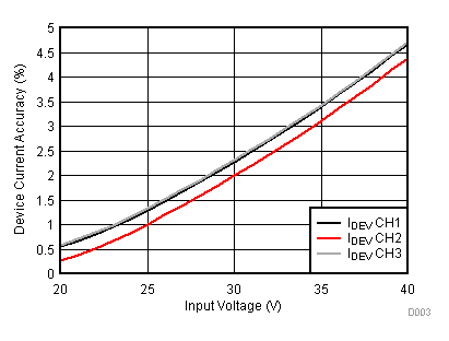
TPS92630-Q1 D003_SLVSC76.gif
V(VIN) = 20 V I(setting) = 150 mA
Figure 3. Device Current Accuracy vs Input Voltage
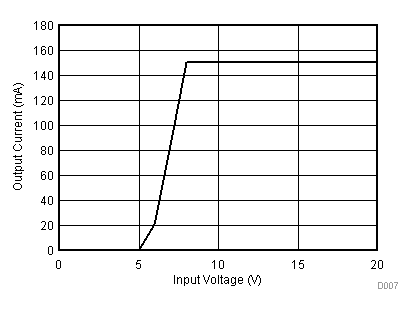
TPS92630-Q1 D007_SLVSC76.gif
3 white LEDs LEDs in series I(setting) = 150 mA
Figure 5. Output Current vs Input Voltage
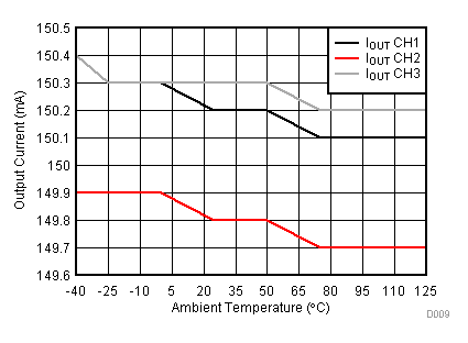
TPS92630-Q1 D009_SLVSC76.gif
I(setting)= 150 mA V(VIN) = 14 V
Figure 7. Output Current vs Ambient Temperature
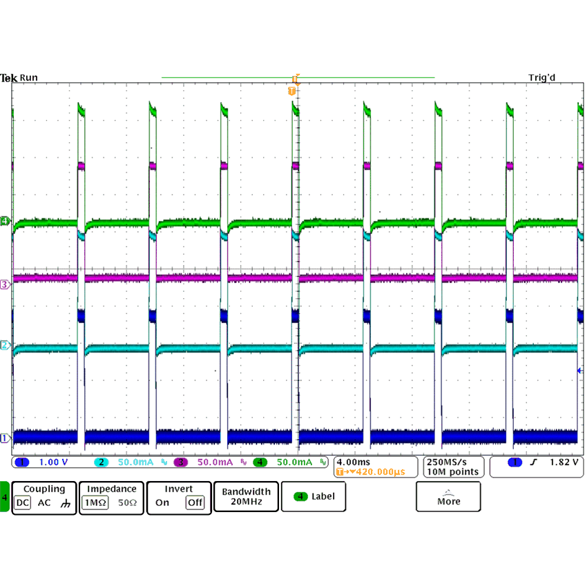
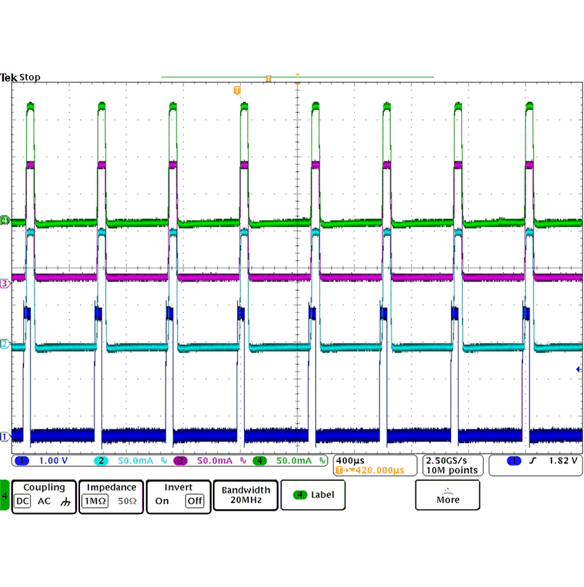
TPS92630-Q1 PWM_200Hz_10Percent_SLVSC76.gif
Ch. 1 = PWM input Ch. 2 = IOUT1 Ch. 3 = IOUT2
Ch. 4 = IOUT3 f(PWM) = 200 Hz Duty cycle = 10%
Figure 9. PWM Dimming
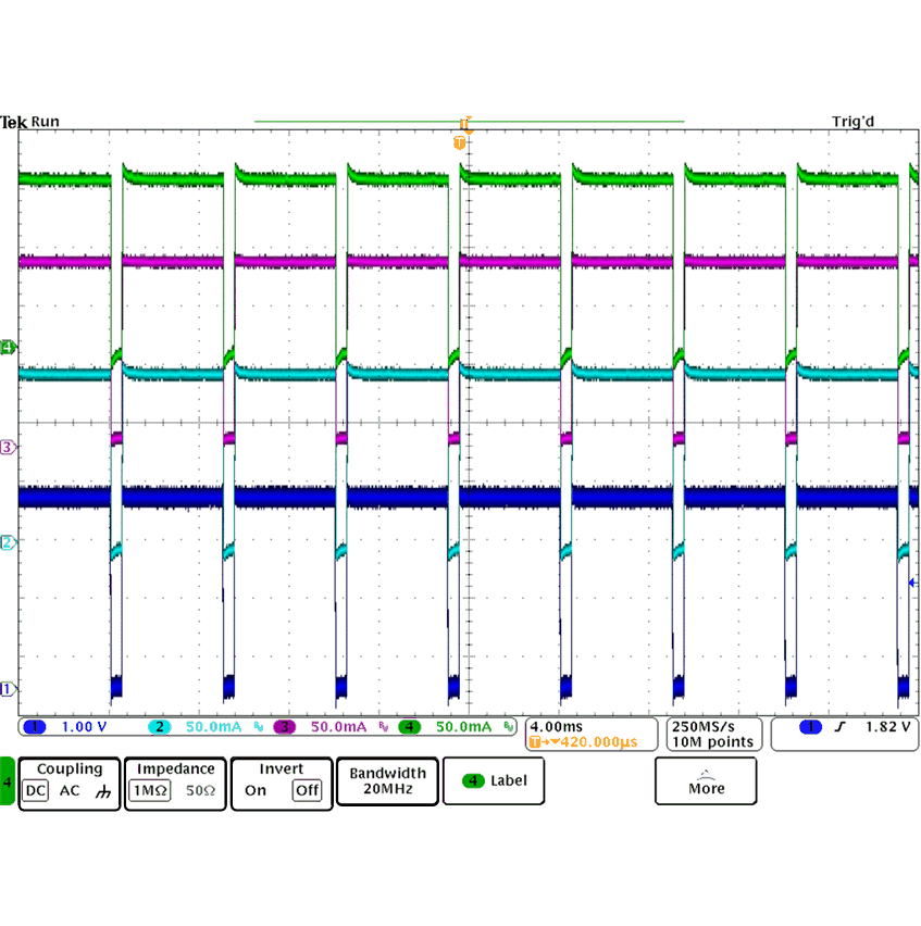
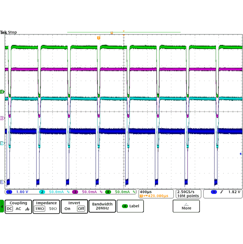
TPS92630-Q1 PWM_200Hz_90Percent_SLVSC76.gif
Ch. 1 = PWM input Ch. 2 = IOUT1 Ch. 3 = IOUT2
Ch. 4 = IOUT3 f(PWM) = 200 Hz Duty cycle = 90%
Figure 11. PWM Dimming
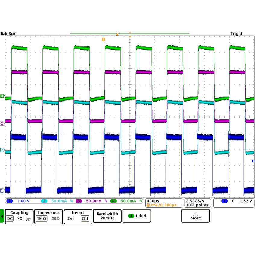
TPS92630-Q1 PWM_2kHz_50Percent_SLVSC76.gif
Ch. 1 = PWM input Ch. 2 = IOUT1 Ch. 3 = IOUT2
Ch. 4 = IOUT3 f(PWM) = 2000 Hz Duty cycle = 50%
Figure 13. PWM Dimming
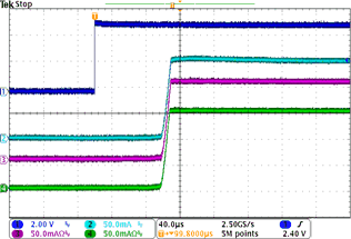
TPS92630-Q1 Power_Up_Waveform_SLVSC76.gif
I(setting) = 60 mA
Figure 15. Fast Power-Up Waveform
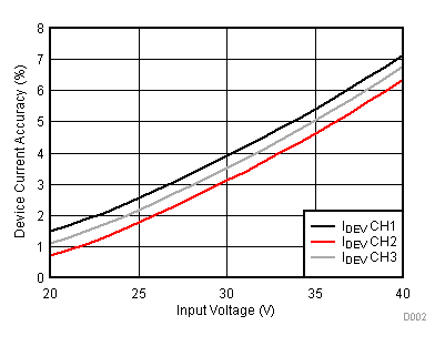
TPS92630-Q1 D002_SLVSC76.gif
V(VIN) = 20 V I(setting) = 30 mA
Figure 2. Device Current Accuracy vs Input Voltage
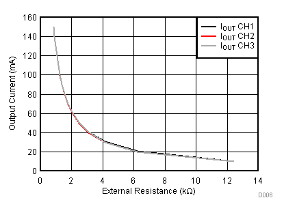
TPS92630-Q1 D006_SLVSC76.gif
A
Figure 4. Output Current vs External Resistance
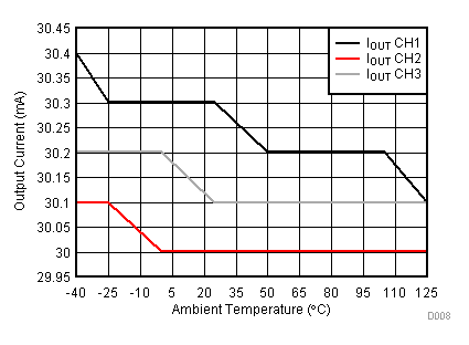
TPS92630-Q1 D008_SLVSC76.gif
I(setting) = 30 mA V(VIN) = 14 V
Figure 6. Output Current vs Ambient Temperature
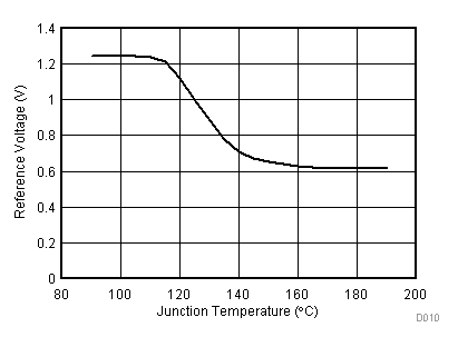
TPS92630-Q1 D010_SLVSC76.gif
A
Figure 8. Reference Voltage vs Junction Temperature With Thermal Foldback
TPS92630-Q1 PWM_200Hz_50Percent_SLVSC76.gif
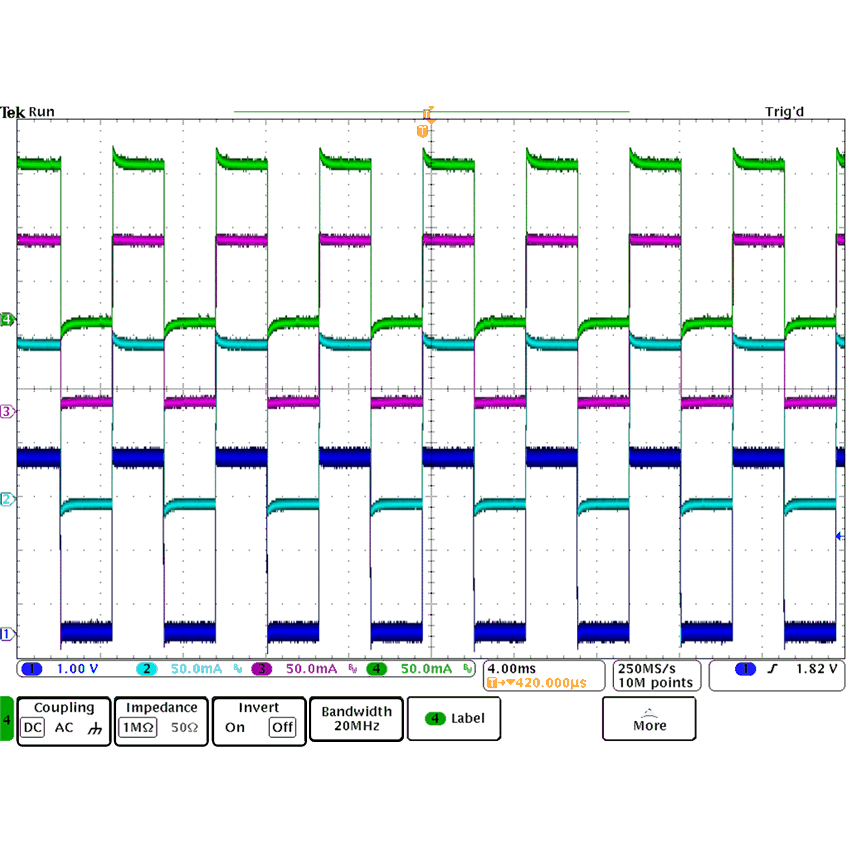
Ch. 1 = PWM input Ch. 2 = IOUT1 Ch. 3 = IOUT2
Ch. 4 = IOUT3 f(PWM) = 200 Hz Duty cycle = 50%
Figure 10. PWM Dimming
TPS92630-Q1 PWM_2kHz_10Percent_SLVSC76.gif
Ch. 1 = PWM input Ch. 2 = IOUT1 Ch. 3 = IOUT2
Ch. 4 = IOUT3 f(PWM) = 2000 Hz Duty cycle = 10%
Figure 12. PWM Dimming
TPS92630-Q1 PWM_2kHz_90Percent_SLVSC76.gif
Ch. 1 = PWM input Ch. 2 = IOUT1 Ch. 3 = IOUT2
Ch. 4 = IOUT3 f(PWM) = 2000 Hz Duty cycle = 90%
Figure 14. PWM Dimming
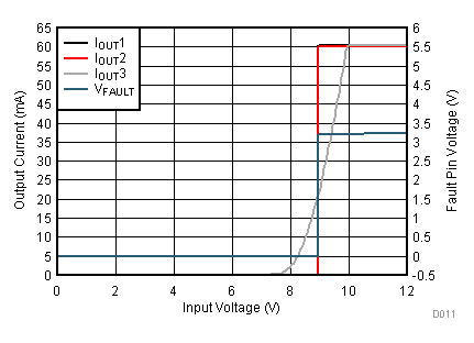
TPS92630-Q1 D011_SLVSC76.gif
V(VIN) = V(EN) V(VIN) = 0 V to 12 V I(setting) = 60 mA
3 white LEDs dV/dt = 0.5 V/min
Figure 16. Slow Power-Up Waveform