SNVS902A October 2012 – October 2015 TPS92640 , TPS92641
PRODUCTION DATA.
- 1 Features
- 2 Applications
- 3 Description
- 4 Revision History
- 5 Pin Configuration and Functions
- 6 Specifications
-
7 Detailed Description
- 7.1 Overview
- 7.2 Functional Block Diagram
- 7.3
Feature Description
- 7.3.1 Controlled On-Time Architecture
- 7.3.2 Switching Frequency
- 7.3.3 Average LED Current
- 7.3.4 Analog Dimming and True-Zero Operation
- 7.3.5 Undervoltage Lockout (UVLO)
- 7.3.6 PWM Dimming Using the UDIM Pin
- 7.3.7 External Shunt FET PWM Dimming
- 7.3.8 VCC Regulation and Start-up
- 7.3.9 Precision Reference
- 7.3.10 Control Loop Compensation
- 7.3.11 Overcurrent Protection
- 7.3.12 Overvoltage Protection (OVP)
- 7.3.13 Boot Undervoltage Lockout (UVLO)
- 7.4 Device Functional Modes
-
8 Application and Implementation
- 8.1 Application Information
- 8.2
Typical Applications
- 8.2.1
TPS92640: Design Procedure
- 8.2.1.1 Design Requirements
- 8.2.1.2
Detailed Design Procedure
- 8.2.1.2.1 Set Output Voltage Feedback Ratio
- 8.2.1.2.2 Set Switching Frequency
- 8.2.1.2.3 Set Average LED Current
- 8.2.1.2.4 Set Inductor Ripple Current
- 8.2.1.2.5 Set LED Ripple Current and Determine Output Capacitance, COUT
- 8.2.1.2.6 Choose N-Channel MOSFETs
- 8.2.1.2.7 Choose Input Capacitance
- 8.2.1.2.8 Set the Turnon Voltage and Undervoltage Lockout Hysteresis
- 8.2.2
TPS92640 - PWM Dimming Application
- 8.2.2.1 Design Requirements
- 8.2.2.2
Detailed Design Procedure
- 8.2.2.2.1 Calculate Operating Points
- 8.2.2.2.2 Output Voltage Feedback
- 8.2.2.2.3 Switching Frequency
- 8.2.2.2.4 Set the Feedback Reference and LED Current
- 8.2.2.2.5 Calculate the Inductor Value
- 8.2.2.2.6 Calculate the Output Capacitor Value
- 8.2.2.2.7 Calculate the MOSFET Parameters
- 8.2.2.2.8 Calculate the Minimum Input Capacitance
- 8.2.2.2.9 Undervoltage Lockout and Hysteresis
- 8.2.2.3 Application Curve
- 8.2.1
TPS92640: Design Procedure
- 9 Power Supply Recommendations
- 10Layout
- 11Device and Documentation Support
- 12Mechanical, Packaging, and Orderable Information
Package Options
Mechanical Data (Package|Pins)
- PWP|16
Thermal pad, mechanical data (Package|Pins)
- PWP|16
Orderable Information
8 Application and Implementation
NOTE
Information in the following applications sections is not part of the TI component specification, and TI does not warrant its accuracy or completeness. TI’s customers are responsible for determining suitability of components for their purposes. Customers should validate and test their design implementation to confirm system functionality.
8.1 Application Information
8.1.1 Switching Frequency
Switching frequency is selected based on the trade-offs between efficiency, solution size/cost and the range of output voltage that can be regulated. Many applications place limits on switching frequency due to EMI sensitiviy. The on-time of the TPS92640 and TPS92641 devices can be programmed for switching frequencies ranging from the tens of kHz to over 1 MHz. This on-time varies in proportion to both VIN and VOUT, as described in Switching Frequency. However, in practice the switching frequency will shift in response to large swings in input or output voltage. The maximum switching frequency is limited only by the minimum on-time and minimum off-time requirements.
8.1.2 LED Ripple Current
The LED manufacturers generally recommend values of current ripple, ΔILED, to achieve optimal optical efficiency. The peak-to-peak current ripple values typically range from ±10% to ±40% of DC current, ILED. Higher LED ripple current allows the use of smaller inductors, smaller output capacitors, or no output capacitors at all. Lower ripple current requires more inductance, higher switching frequency, or additional output capacitance. Based on the LED current ripple specification and desired switching frequency, the inductor value can be calculated using Equation 13.

It is important to ensure that the rated inductor saturation current is greater than the worst case operating current (ILED+ΔILED/2) under the wide operating temperature range.
8.1.3 Buck Converters Without Output Capacitor
A Buck regulator is ideal for regulating current because of the direct connection between the inductor and the LED load. Because the current is being regulated, not voltage, a buck current regulator is free of load current transients, and has no need of output capacitance to supply the load and maintain output voltage. This is of great benefit when driving LEDs as large electrolytic capacitors impact the lifetimes and PWM dimming performance. The output capacitor can be eliminated by using a large inductor or higher switching frequency as discussed in LED Ripple Current
A capacitor placed in parallel with the LED or array of LEDs can be used to reduce ΔiLED while keeping the same average current through both the inductor and the LED array. With this topology the inductance can be lowered, making the magnetics smaller and less expensive. Alternatively, the circuit can be run at lower frequency with the same inductor value, improving the efficiency and expanding the range of output voltage that can be regulated.
Figure 22 shows the equivalent impedances presented to the ΔiL-PP when an output capacitor, COUT, and its equivalent series resistance (RESR) are placed in parallel with the LED array.
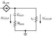 Figure 22. LED Ripple Current With COUT
To calculate the respective ripple currents, the LED array is represented as the dynamic resistance, (rD). LED's dynamic resistance is not always specified on the manufacturer’s data sheet, but it can be calculated as the inverse slope of the LED’s VLED vs ILED curve at the operating point. However, this method only gives an rough estimate of rD. Total dynamic resistance for a string of n LEDs connected in series can be calculated as the rD of one device multiplied by n. Inductor ripple current, ΔiL-PP is still calculated as before. The following equations can then be used to estimate peak-to-peak LED current ripple, ΔiLED-PP, when using a parallel capacitor:

The calculation for ZCOUT assumes that the shape of the inductor ripple current is approximately sinusoidal. Small values of COUT that do not significantly reduce ΔiLED-PP can also be used to control EMI generated by the switching action of the TPS92640 and TPS92641 devices. EMI reduction becomes more important as the length of the connections between the LED and the rest of the circuit increase.
8.1.4 Input Capacitor
Input capacitor is selected using requirements for minimum capacitance and rms ripple current. The input capacitor supply pulses of current approximately equal to ILED while the high-side NFET is on, and is charged up by the input voltage while the high-side NFET is off. Switching converters such as the TPS92640 and TPS92641 devices have a negative input impedance due to the decrease in input current as input voltage increases. This inverse proportionality of input current to input voltage can cause oscillations (sometimes called power supply interaction) if the magnitude of the negative input impedance is greater than the input filter impedance. Minimum capacitance can be selected by comparing the input impedance to the converter’s negative resistance; however, this requires accurate calculation of the input voltage source inductance and resistance, quantities which can be difficult to determine. An alternative method to select the minimum input capacitance (CIN-MIN) is to select the maximum voltage ripple (ΔvIN-MAX), which can be tolerated. ΔvIN-MAX is equal to the change in voltage across CIN during tON when it supplies the load current. A good starting point for selection of CIN is to use an input voltage ripple of 2% to 10% of VIN. CIN-MIN can be selected using Equation 15.

TI recommends a minimum input capacitance at least 75% greater than the CIN-MIN value. To determine the RMS input current rating (IIN-RMS), use Equation 16.

Because this approximation assumes there is no inductor ripple current, the value should be increased by 10-30% depending on the amount of ripple that is expected. Ceramic capacitors are the best choice for the input to the TPS92640 and TPS92641 devices due to their high ripple current rating, low ESR, low cost, and small size compared to other types. When selecting a ceramic capacitor, special attention must be paid to the operating conditions of the application. Ceramic capacitors can lose one-half or more of their capacitance at their rated DC voltage bias and also lose capacitance with extremes in temperature. Make sure to check any recommended deratings and also verify if there is any significant change in capacitance at the operating input voltage and the operating temperature.
8.1.5 NFETs
The TPS92640 and TPS92641 devices require two external NFETs for the switching regulator. The FETs should have a voltage rating at least 20% higher than the maximum input voltage to ensure safe operation during the ringing of the switch node. In practice, all switching converters have some ringing at the switch node due to the diode parasitic capacitance and the lead inductance. The NFETs should also have a current rating at least 50% higher than the average transistor current. Once NFETs are chosen, the power rating is verified by calculating the power loss.
8.2 Typical Applications
8.2.1 TPS92640: Design Procedure
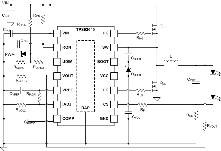 Figure 23. TPS92640 Design Procedure Schematic
8.2.1.1 Design Requirements
- VIN
- VLED
- Number of LEDs in Series
- ILED
- fSW
- VCS
- ΔiLED-PP
- ΔVIN-PP
- VTURN-ON
- VHYS
8.2.1.2 Detailed Design Procedure
8.2.1.2.1 Set Output Voltage Feedback Ratio
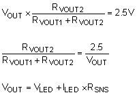
For the desired output (VOUT), RVOUT1 and RVOUT2 is calculated first with the desired feedback voltage, VVOUT at approximately 2.5 V:
8.2.1.2.2 Set Switching Frequency
The switching frequency is set as follows:

8.2.1.2.3 Set Average LED Current
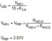
The average LED current (ILED) is set by:
8.2.1.2.4 Set Inductor Ripple Current
First, the expected duty cycle, D must be determined:

With the inductor ripple current, ΔiL-PP specified and the expected duty cycle, the inductance (L) can be chosen:

8.2.1.2.5 Set LED Ripple Current and Determine Output Capacitance, COUT
The LED ripple current (ΔiLED-PP ) is specified. With the target ripple current determined, the output capacitance (COUT) can be chosen using Equation 22.

8.2.1.2.6 Choose N-Channel MOSFETs
The suggested minimum voltage rating, VT-MAX and current rating, IT-MAX are:

Selecting a proper power MOSFET is critical in a power application, other than the SOA limits, the gate characteristic and the RDSON can affect the system performance seriousely.
Also, the peak current limit (ILIMIT) is governed by:
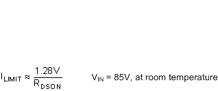
Both the current limit threshold and MOSFET RDSON are loosely specified and can vary a lot with temperature, input voltage and other operating conditions.
8.2.1.2.7 Choose Input Capacitance
Input capacitance is necessary to provide instantaneous current to the discontinuous portions of the circuit during the high side NFET on-time. The allowable input voltage ripple (ΔvIN-PP) is specified at approximately 3% Pk-Pk of VIN. The minimum required capacitance (CIN_MIN) to achieve this specification is:

The necessary RMS input current rating (IIN-RMS) can be approximated as follows:

8.2.1.2.8 Set the Turnon Voltage and Undervoltage Lockout Hysteresis
With the desired turnon threshold voltage (VTURN_ON) stated, the resistor divider network composing with RUDIM1 and RUDIM2 can be calculated with the equation in below.
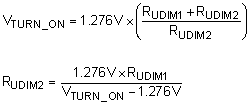
Then RUDIM3 is optional and recommended for PWM. The RUDIM3 can be calculated based on Equation 10 to provide the desired undervoltage lockout hysteresis (VHYS).
8.2.2 TPS92640 – PWM Dimming Application
 Figure 24. PWM Dimming Using UDIM Pin Schematic
8.2.2.1 Design Requirements
- VIN = 48 V ± 10%
- VLED = 3.25 V, 325-mΩ dynamic resistance
- 10 LEDs in Series, rD = 3.25 Ω
- ILED = 1 A
- fSW = 500 kHz
- VCS = 200 mV
- ΔiLED-PP ≤ 300 mA
- ΔVIN-PP ≤ 1.5 V
- VTURN-ON = 40 V
- VHYS = 15 V
8.2.2.2 Detailed Design Procedure
8.2.2.2.1 Calculate Operating Points
Calculate the operating points using Equation 28 to Equation 30, and assume approximately 90% conversion efficiency (η = 0.9).


8.2.2.2.2 Output Voltage Feedback
Calculate the VOUT pin resistors by setting RVOUT2 = 10 kΩ and calculating RVOUT1.

Choose RVOUT1 = 120 kΩ.
8.2.2.2.3 Switching Frequency
Using the values calculated above choose a value of CON = 1 nF and calculate the value of RON:

Choose the closest standard resistor value of RON = 26.1 kΩ.
8.2.2.2.4 Set the Feedback Reference and LED Current
To get a value of VCS = 200 mV VIADJ must be set to 2 V. Choose a value of RIADJ1 = 10 kΩ and solve for RIADJ2:

Choose the standard resistor value of RIADJ2 = 19.6 kΩ and solve for RCS using Equation 34.

RCS = 0.2 Ω is a standard resistor value.
8.2.2.2.5 Calculate the Inductor Value
Because this is a PWM dimming application, TI does not recommend much output capacitance for faster current rise and fall times, so the inductor ripple current should be close to the 300-mA peak-to-peak LED ripple current. Calculate and inductor value that will give you 350-mA peak-to-peak inductor ripple current or less:

Choose the standard value of L = 68 µH which results in an actual ΔiL-PP of 342 mA.
8.2.2.2.6 Calculate the Output Capacitor Value
Given the actual inductor ripple current of 342-mA peak-to-peak, use Equation 36 to calculate the required output capacitor value.

Choose COUT = 0.1 µF.
8.2.2.2.7 Calculate the MOSFET Parameters
The MOSFETs must have a minimum voltage and current rating for the application. The minimum ratings are calculated using Equation 37 and Equation 38.


Choose MOSFETs that have a drain-to-source voltage rating of greater than 63 V and a current rating greater than 1.26 A.
8.2.2.2.8 Calculate the Minimum Input Capacitance
The minimum input capacitance to achieve 1.5-V peak-to-peak input voltage ripple is calculated using Equation 39.

For PWM dimming applications more input voltage ripple will be present at the PWM dimming frequency. For these applications, TI recommends using 10 times the amount of minimum input capacitance or more. Choose CIN = 10 µF.
8.2.2.2.9 Undervoltage Lockout and Hysteresis
Choose a value of RUDIM1 = 100 kΩ and calculate the values of RUDIM2 and RUDIM3 using Equation 40 and Equation 41.


Choose the nearest standard resistor values of RUDIM2 = 3.32 kΩ and RUDIM3 = 19.1 kΩ.
8.2.2.3 Application Curve
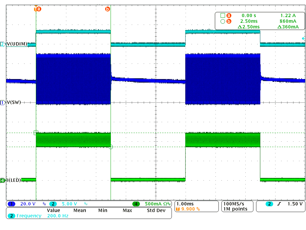 Figure 25. UDIM Dimming Waveform