SLASE37A May 2014 – December 2014 TRF37A32 , TRF37B32 , TRF37C32
PRODUCTION DATA.
- 1 Features
- 2 Applications
- 3 Description
- 4 Simplified Schematic
- 5 Revision History
- 6 Pin Configuration and Functions
-
7 Specifications
- 7.1 Absolute Maximum Ratings
- 7.2 ESD Ratings
- 7.3 Recommended Operating Conditions
- 7.4 Thermal Information
- 7.5 Electrical Characteristics, TRF37A32
- 7.6 Electrical Characteristics, TRF37B32
- 7.7 Electrical Characteristics, TRF37C32
- 7.8 Timing Requirements
- 7.9 Typical Characteristics (TRF37A32)
- 7.10 Typical Characteristics (TRF37B32)
- 7.11 Typical Characteristics (TRF37C32)
- 8 Detailed Description
- 9 Applications and Implementation
- 10Power Supply Recommendations
- 11Layout
- 12Device and Documentation Support
Package Options
Mechanical Data (Package|Pins)
- RTV|32
Thermal pad, mechanical data (Package|Pins)
- RTV|32
Orderable Information
8 Detailed Description
8.1 Overview
The TRF37x32 family is a dual-channel, down convert receive mixer. It provides high-linearity over wide RF and IF bandwidths while also consuming low power. The device comes in three varieties, A, B, and C, to cover an extremely wide frequency band and can operate with either low side injection (LSI) or high side injection (HSI). The IF output is optimized for 200 MHz but operates from 30 MHz to 600 MHz with appropriate external components.
The device consists of a passive mixer core buffered by an LO amplifier and a high-linearity IF amplifier. There is an on-chip LDO to regulate VCC to the voltages needed for the small-geometry SiGe BiCMOS components. The single-ended RF and LO inputs each have a wideband internal balun. The balun's center tap is internally grounded.
Each channel offers an external power down terminal control which disables the IF circuitry. The device has a low power mode controlled through an external terminal control. Low power mode reduces bias current in the LO circuitry. Both power down and low power mode controls are internally biased to a normal operating state. The IFA/B_BT terminals are self-biased and require no external components.
The TRF37x32 uses a single 3.3 V power supply and draws exceptionally low current for its performance node.
8.2 Functional Block Diagram
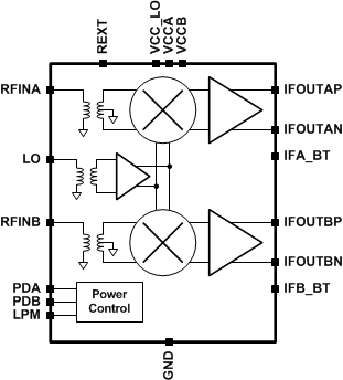 Figure 73. Block Diagram
8.3 Feature Description
8.3.1 Low Power Mode
Low power mode is enabled by setting the active-high LPM terminal to a logic high. The device contains an internal pull-down to engage normal operation when the terminal is left unconnected or floating.
Low power mode reduces the bias current in the LO amplifier portion of the device and affects both channels. Total current consumption is reduced 30% while lowering analog performance metrics.
8.3.2 Power Down
Each channel is powered down individually through the active-high PDA and PDB terminals. A logic high sets the respective channel in power down. The device contains an internal pull-down to engage normal operation when the terminal is left unconnected or floating.
Power down is implemented by removing bias in the IF amplifier. Operation of the opposite channel is not affected when either channel is turned off. Turn-on and turn-off time is fast enough to serve in most TDD applications.
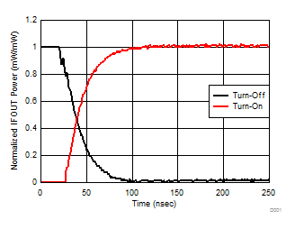 Figure 74. Device power down turn-on and turn-off time
8.3.3 Single Ended RF Input
Each RF input is single-ended with a wideband internal balun to convert the input to a differential signal, as shown in Figure 73. The center tap of the balun is internally grounded and is not available external to the device. The RF input should be ac coupled to driving circuitry according to the chart in Table 1.
Table 1. RF Input AC coupling capacitor
| Device | Blocking Cap Value |
|---|---|
| TRF37A32 | 20 pF |
| TRF37B32 | 10 pF |
| TRF37C32 | 10 pF |
8.3.4 Single Ended LO Input
The LO input is single ended with an internal balun to convert the input to a differential signal. The LO drive path includes a high frequency dual-mode oscillation inhibitor circuitry to ensure stable operation. For best operation it is recommended to keep the LO drive level at 0 dBm or higher to ensure inhibitor circuit does not falsely engage. At lower LO drive level, keep the LO power engaged to the device at power-up. At lower drive level the inhibitor may engage within certain frequency bands when the LO power transitions.
At the extreme RF frequencies the LO input bandwidth will force operation to either high side injection (HSI) or low side injection (LSI). Table 2 provides the operating range of the LO for each device.
Table 2. LO Input Frequency Operating Range
| Device | Operating Range | |
|---|---|---|
| TRF37A32 | 600 - 1400 MHz | |
| TRF37B32 | 500 - 2900 MHz | |
| TRF37C32 | Low Power mode (LPM) disabled | 1500 - 3600 MHz |
| Low Power mode (LPM) enabled | 1500 - 3500 MHz | |
8.3.5 IF Amplifier
The output of the device is driven by a high-linearity IF amplifier. The output nodes must be pulled up to VCC with high-Q inductors. It is designed to provide 200 Ω differential / 100 Ω single-ended output impedance. Layout should include symmetry for the differential output signal paths.
The IF output circuitry is optimized for performance at 200 MHz but operates over 30 MHz – 600 MHz.
8.4 Device Functional Modes
8.4.1 Low Power Mode
Low power mode is activated through the low power terminal, as described in the features description. It is designed for extremely low power consumption.
8.4.2 Single Channel and Shutdown Modes
The device may be operated as a single channel device by disabling one channel or in complete shutdown by disabling both channels.