SLASE37A May 2014 – December 2014 TRF37A32 , TRF37B32 , TRF37C32
PRODUCTION DATA.
- 1 Features
- 2 Applications
- 3 Description
- 4 Simplified Schematic
- 5 Revision History
- 6 Pin Configuration and Functions
-
7 Specifications
- 7.1 Absolute Maximum Ratings
- 7.2 ESD Ratings
- 7.3 Recommended Operating Conditions
- 7.4 Thermal Information
- 7.5 Electrical Characteristics, TRF37A32
- 7.6 Electrical Characteristics, TRF37B32
- 7.7 Electrical Characteristics, TRF37C32
- 7.8 Timing Requirements
- 7.9 Typical Characteristics (TRF37A32)
- 7.10 Typical Characteristics (TRF37B32)
- 7.11 Typical Characteristics (TRF37C32)
- 8 Detailed Description
- 9 Applications and Implementation
- 10Power Supply Recommendations
- 11Layout
- 12Device and Documentation Support
Package Options
Mechanical Data (Package|Pins)
- RTV|32
Thermal pad, mechanical data (Package|Pins)
- RTV|32
Orderable Information
11 Layout
11.1 Layout Guidelines
Good layout practice helps to enable excellent linearity and isolation performance. An example of good layout is shown in Figure 78. In the example, only the top signal layer and its adjacent ground reference plane are shown. Some recommended layout principles include the following:
- Excellent electrical connection from the PowerPAD™ to the board ground is essential. Use the recommended footprint, solder the pad to the board, and do not include solder mask under the pad
- Connect pad ground to device terminal ground on the top board layer.
- Verify that the return current path follows the primary current path by including topside terminal to pour ground connection and vias close to any reference layer transition.
- Do not route signal lines over breaks in the reference plane.
- Maintain symmetry as much as possible between lines in a differential pair. Match electrical lengths.
- Avoid routing clocks and digital control lines near signal lines.
- Do not route signal lines over noisy power planes. Ground is the best reference, although clean power planes can serve where necessary.
- Place supply decoupling close to the device.
- Keep channels physically separated to improve isolation.
11.2 Layout Example
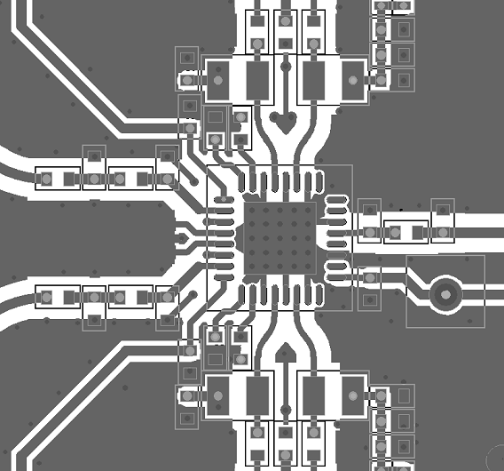 Figure 78.