SLLSF63B March 2018 – October 2023 TUSB1002A
PRODUCTION DATA
- 1
- 1 Features
- 2 Applications
- 3 Description
- 4 Revision History
- 5 Pin Configuration and Functions
- 6 Specifications
-
7 Detailed Description
- 7.1 Overview
- 7.2 Functional Block Diagram
- 7.3
Feature Description
- 7.3.1 4-Level Control Inputs
- 7.3.2 Linear Equalization
- 7.3.3 Adjustable VOD Linear Range and DC Gain
- 7.3.4 USB3.2 Dual Channel Operation (MODE = “F”)
- 7.3.5 USB3.2 Single Channel Operation (MODE = “1”)
- 7.3.6 PCIe/SATA/SATA Express Redriver Operation (MODE = “R”; CFG1 = "0"; CFG2 = "0" )
- 7.3.7 Basic Redriver Operation (MODE = “0”)
- 7.4 Device Functional Modes
- 7.5 U0 Mode
- 7.6 U1 Mode
- 7.7 U2/U3 Mode
- 8 Application and Implementation
- 9 Device and Documentation Support
- 10Mechanical, Packaging, and Orderable Information
Package Options
Refer to the PDF data sheet for device specific package drawings
Mechanical Data (Package|Pins)
- RGE|24
Thermal pad, mechanical data (Package|Pins)
- RGE|24
Orderable Information
3 Description
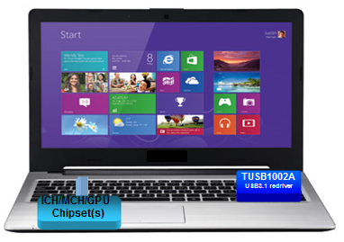
The TUSB1002A is the industry’s first dual-channel USB 3.2 x1 SuperSpeedPlus (SSP) redriver and signal conditioner. The device offers low power consumption on a 3.3-V supply with its ultra-low-power architecture. It supports the USB3.2 low power modes which further reduces idle power consumption.
The TUSB1002A implements a linear equalizer, supporting up to 16 dB of loss due to inter-symbol interference (ISI). When USB signals travel across a PCB or cable, signal integrity degrades due to loss and inter-symbol interference. The linear equalizer compensates for the channel loss, and thereby, extends the channel length and enables systems to pass USB compliance. The dual lane implementation and small package size provides flexibility in the placement of the TUSB1002A in the USB3.2 path.
The TUSB1002A is available in either a 24-pin 4 mm × 4 mm VQFN. It is also available in a commercial grade (TUSB1002A) or industrial grade (TUSB1002AI).
| PART NUMBER(1) | TEMPERATURE | PACKAGE |
|---|---|---|
| TUSB1002A | TA = 0°C to 70°C | RGE (VQFN, 24) |
| TUSB1002AI | TA = -40°C to 85°C |
 Simplified Schematic