SLASE51A November 2014 – November 2014 TVB1440
PRODUCTION DATA.
- 1 Features
- 2 Applications
- 3 Description
- 4 Simplified Schematics
- 5 Revision History
- 6 Pin Configuration and Functions
- 7 Specifications
- 8 Detailed Description
- 9 Application and Implementation
- 10Power Supply Recommendations
- 11Layout
- 12Device and Documentation Support
- 13Mechanical, Packaging, and Orderable Information
Package Options
Mechanical Data (Package|Pins)
- RGZ|48
Thermal pad, mechanical data (Package|Pins)
- RGZ|48
Orderable Information
9 Application and Implementation
NOTE
Information in the following applications sections is not part of the TI component specification, and TI does not warrant its accuracy or completeness. TI’s customers are responsible for determining suitability of components for their purposes. Customers should validate and test their design implementation to confirm system functionality.
9.1 Application Information
TVB1440 is a signal conditioner especially suited for equalizing channel loss due to traces and flexible cable between digital TV chipset and TCON receiver.
9.1.1 Typical Application
The device can be helpful improving eye diagram by placing it either end of the flexible cable in digital TV chipset or TCON board or at the both. Figure 9 shows a typical application for TV interface.
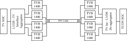 Figure 9. Typical Application of TVB1440 in 4K2K Digital TV Interface
9.1.1.1 Design Requirements
Table 5. Design Parameters
| PARAMETER | VALUE |
|---|---|
| VDD Supply | 1.1 V |
| VCC Supply | 3.3 V |
| TV Max Resolution Requirement | |
| Pixel Clock (MHz) | 1194 |
| Horizontal Active (pixels) | 3840 |
| Vertical Active | 2160 |
| Color bit Depth (6bpc, 8bpc, 10bpc) | 10 (30 bpp) |
| Refresh Rate | 120 Hz |
| Panel Configuration (A or B) | B |
| Channel Requirements | |
| Input Channel Insertion Loss | Up to 12 dB at 3.75 Gbps |
| Output Channel Insertion Loss | Up to 12 dB at 3.75 Gbps |
| TVB1440 Settings | |
| Number of Lanes (1, 2, or 4) | 4 |
| Link Rate (Gbps) | 3.75 |
| RX EQ Setting (dB) | 6.5 dB |
| TX VOD Setting (Level 0, 1, 2, or 3) | Level 3 (1000 mVpp) |
| TX Pre-Emphasis Setting (Level 0, 1, 2, or 3) | Level 0 (0 dB) |
9.1.1.2 Detailed Design Procedure
9.1.1.2.1 Common 4k2k TV Panel Configuration
A common 4k2k TV is broken into four 1920 x 1080 panels or four 960 x 2160 panels. For this particular implementation, panel configuration B is assumed. It is also assumed that two TVB1440 are used for each panel (one near SOC and one near TCON) for a total of eight TVB1440.
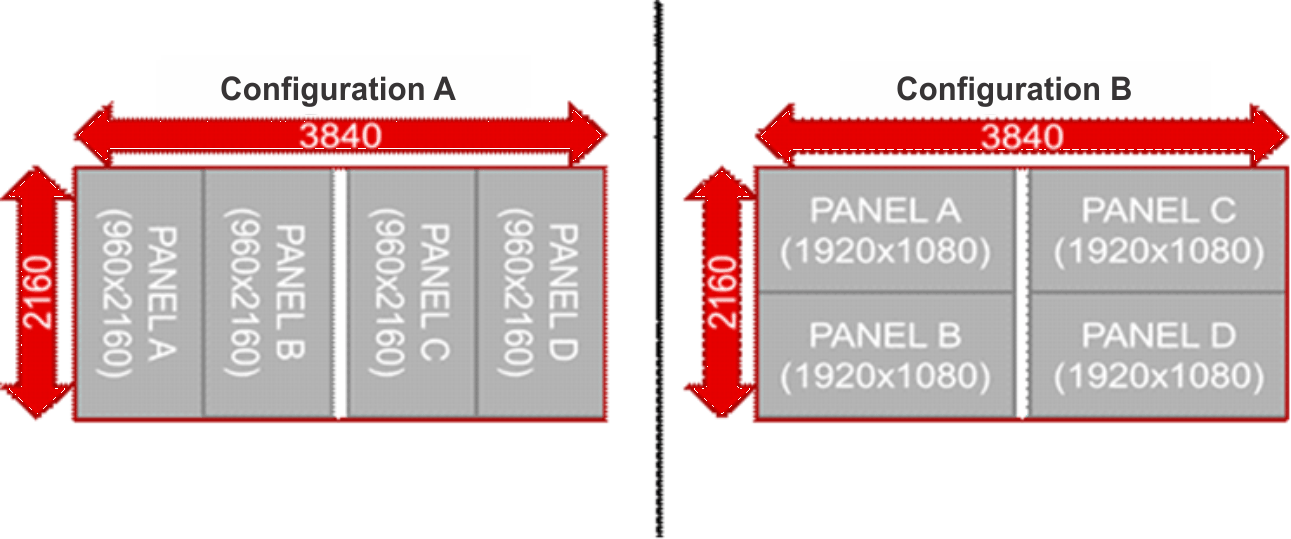 Figure 10. Common Panel Configurations
9.1.1.2.2 1Max Stream Rate
The maximum stream rate can be derived from the maximum TV resolutions pixel clock and color depth. For this example, the maximum pixel clock is 1194 MHz. Because the TV is broken into 4 panels, the actual pixel clock for each panel is 298.5 MHz.
Stream Bit Rate = PixelClock x bpp
Stream Bit Rate = 298.5 x 30
Stream Bit Rate = 8.955 Gbps.
9.1.1.2.3 Encoded Stream Rate
Most high-speed video standards are 8b10b encoded. Because of 8b10b encoding overhead, an additional 20% must be added to the stream bit rate. On top of the 8b10b, there are some additional overhead due to packetization before the 8b10b encode that also must be added to the stream bit rate. For example, a particular video standard may define the actual coded stream rate by the following equation.
Encoded_Stream_Rate = #_of_Bytes_for_bpp x 8 x 1.25 x PixelClock
Encoded_Stream_Rate = #_of_Bytes_for_bpp x 8 x 1.25 x PixelClock
Encoded_Stream_Rate = 11.94Gbps.
9.1.1.2.4 TVB1440 Configuration
The TVB1440 must be configured by the SOC using I2C. Because of the limited number of I2C address available on the TVB1440, an I2C switch needs to be incorporated in order to configure each of the TVB1440. Figure 11 shows an example implement using the Texas Instruments TCA9546A 4-channel I2C switch.
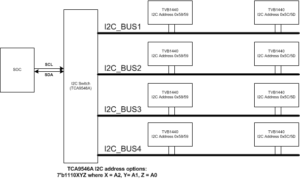 Figure 11. Example I2C Switch Implementation
9.1.1.2.5 Receiver Equalization Setting
The TVB1440 has a receiver equalizer that is adjustable from 0dB to 15 dB at 5 Gbps. The common approach to determine the proper equalizer setting is to measure the insertion loss of the channel at the input of the TVB1440 at the Nyquist frequency of the data rate (1.875 GHz for 3.75 Gbps and 2.5 GHz for 5 Gbps). For example, if the input channel is 20 inches of trace with 4 mil width over FR4, the insertion loss at 3.75 Gbps would be -7.3 dB and at 5 Gbps would be -9.1 dB. The register EQ_LEVEL_LANEx, where X = 0, 1, 2, or 3 should be programmed to 3’b100 for a 3.75 Gbps data rate and should be programmed to 3’b101. The actual setting may need to be adjusted based on the additional channel parasitics from package, vias, and connectors.
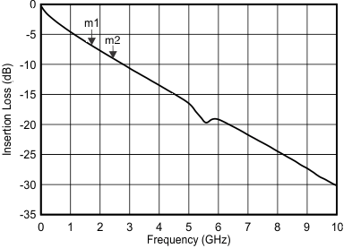
| m1 frequency = 1.876 GHz | IL = –7.346 | |||
| m2 frequency = 2.500 GHz | IL = –9.185 |
9.1.1.2.6 Transmitter Settings
The TVB1440’s transmitter controls have four settings for voltage swing and four settings for pre-emphasis. The best transmitter setting to use is a function of the output channel insertion loss and the inputs eye requirement of the device at end of the channel. For the case in which a TVB1440 is at the end of the channel, the output channel’s insertion loss should not be greater than the receiver equalization of the TVB1440.
To specify the largest eye opening at the end of the channel, the best voltage swing setting should be either level 2 or level 3. It is also recommended to use either a pre-emphasis level of 0 dB or 3dB. The pre-emphasis setting can be thought of as a way to reduce the amount receiver equalizer required by the device at end channel. For example, a 3.5dB setting could allow for the receive equalization setting for the TVB1440 to be reduced from 12dB to 10dB. If necessary, these settings can be adjusted up or down in order to improve the eye opening at the end of the channel.
9.1.1.2.7 RESET
The TVB1440 RSTN input gives control over the device reset and to place the device into shut-down mode. When RSTN is low, all registers are reset to their default values, which means all HS Link ports are disable. When the RSTN pin is released back to high, the device comes out of the shut-down mode. To turn on the HS Link, it is necessary to provision the device registers through the local I2C_CTL interface.
It is critical to transition the RSTN input from a low to a high level after both VCC and VDD supply voltages have reached the minimum recommended operating voltage. This is achieved by a control signal to the RSTN input, or by an external capacitor connected between RSTN and GND. To insure that the TVB1440 is properly reset, the RSTN pin must be de-asserted for at least 100 μs before being asserted.
The RSTN input includes a 150k resistor from the input to the VDD supply. An external capacitor connected between RSTN and GND allows delaying the RSTN signal during power up. When implementing the external capacitor the size of the external capacitor depends on the power up ramp of the VCC and VDD supplies; a slower ramp-up results in a larger value external capacitor. Approximately 200 nF capacitor is a reasonable first estimate for the size of the external capacitor for most applications.
Both RSTN implementations are shown in Figure 13.
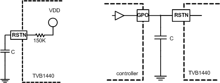 Figure 13. (a) Reset Implementation Using a Capacitor, (b) Microprocessor Drives the Pin
Figure 14 shows a typical schematic implementation either in TV chipset or TCONS receiver board.
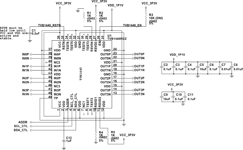 Figure 14. Schematic Implementation of TVB1440