SLASE51A November   2014  – November 2014 TVB1440

PRODUCTION DATA.  

  1. Features
  2. Applications
  3. Description
  4. Simplified Schematics
  5. Revision History
  6. Pin Configuration and Functions
  7. Specifications
    1. 7.1 Absolute Maximum Ratings
    2. 7.2 Handling Ratings
    3. 7.3 Recommended Operating Conditions
    4. 7.4 Thermal Information
    5. 7.5 Electrical Characteristics
    6. 7.6 Timing Requirements
    7. 7.7 Switching Characteristics
    8. 7.8 Typical Characteristics
  8. Detailed Description
    1. 8.1 Overview
    2. 8.2 Functional Block Diagram
    3. 8.3 Feature Description
      1. 8.3.1 Equalization
      2. 8.3.2 Configurable Output
      3. 8.3.3 Squelch
    4. 8.4 Device Functional Modes
      1. 8.4.1 Active Mode
      2. 8.4.2 Shutdown Mode
      3. 8.4.3 Squelch Mode
    5. 8.5 Programming
      1. 8.5.1 Local I2C Interface
      2. 8.5.2 Receiver (IN[3:0]P/N) Adjustments
        1. 8.5.2.1 Equalization Level
        2. 8.5.2.2 Squelch Level
      3. 8.5.3 Main Link Output [OUT[3:0]P/N] Adjustments
        1. 8.5.3.1 LINK Address Space
      4. 8.5.4 Example Script
    6. 8.6 Register Maps
  9. Application and Implementation
    1. 9.1 Application Information
      1. 9.1.1 Typical Application
        1. 9.1.1.1 Design Requirements
        2. 9.1.1.2 Detailed Design Procedure
          1. 9.1.1.2.1 Common 4k2k TV Panel Configuration
          2. 9.1.1.2.2 1Max Stream Rate
          3. 9.1.1.2.3 Encoded Stream Rate
          4. 9.1.1.2.4 TVB1440 Configuration
          5. 9.1.1.2.5 Receiver Equalization Setting
          6. 9.1.1.2.6 Transmitter Settings
          7. 9.1.1.2.7 RESET
  10. 10Power Supply Recommendations
    1. 10.1 Power-Up Sequence
    2. 10.2 Power-Down Sequence
  11. 11Layout
    1. 11.1 Layout Guidelines
      1. 11.1.1 Differential Pairs
      2. 11.1.2 Layout Example
      3. 11.1.3 Placement
      4. 11.1.4 Package Specific
      5. 11.1.5 Ground
  12. 12Device and Documentation Support
    1. 12.1 Trademarks
    2. 12.2 Electrostatic Discharge Caution
    3. 12.3 Export Control Notice
    4. 12.4 Glossary
  13. 13Mechanical, Packaging, and Orderable Information

Package Options

Mechanical Data (Package|Pins)
Thermal pad, mechanical data (Package|Pins)
Orderable Information

10 Power Supply Recommendations

The following power-up and power-down sequences describe how the RSTN signal is applied to the TVB1440.

10.1 Power-Up Sequence

  1. Apply VDD then VCC (recommended both less than 10-ms ramp time). VDD must be asserted first and stable for greater than 10 μs before VCC is applied.
  2. RSTN must remain asserted until VCC/VDD voltage has reached minimum recommended operation for more than 100 μs.
  3. De-assert RSTN (Note: This RSTN is a 1.1V interface and is internally connected to VDD through a 150-kΩ resistor).
  4. Device will be available for operation approximately 400 ms after a valid reset.
power_up_sequence_slase51.gif
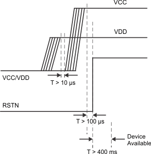
Figure 15. Power-up Sequence

10.2 Power-Down Sequence

There is no power-down sequence required.