SCES641E May 2007 – October 2023 TXB0102
PRODUCTION DATA
- 1
- 1 Features
- 2 Applications
- 3 Description
- 4 Pin Configuration and Functions
-
5 Specifications
- 5.1 Absolute Maximum Ratings
- 5.2 ESD Ratings
- 5.3 Recommended Operating Conditions
- 5.4 Thermal Information
- 5.5 Electrical Characteristics: TA = 25°C
- 5.6 Electrical Characteristics: TA = –40°C to +85°C
- 5.7 Operating Characteristics
- 5.8 VCCA = 1.2 V Timing Requirements
- 5.9 VCCA = 1.5 V ± 0.1 V Timing Requirements
- 5.10 VCCA = 1.8 V ± 0.15 V Timing Requirements
- 5.11 VCCA = 2.5 V ± 0.2 V Timing Requirements
- 5.12 VCCA = 3.3 V ± 0.3 V Timing Requirements
- 5.13 VCCA = 1.2 V Switching Characteristics
- 5.14 VCCA = 1.5 V ± 0.1 V Switching Characteristics
- 5.15 VCCA = 1.8 V ± 0.15 V Switching Characteristics
- 5.16 VCCA = 2.5 V ± 0.2 V Switching Characteristics
- 5.17 VCCA = 3.3 V ± 0.3 V Switching Characteristics
- 5.18 Typical Characteristics
- 6 Parameter Measurement Information
- 7 Detailed Description
- 8 Application and Implementation
- 9 Device and Documentation Support
- 10Revision History
- 11Mechanical, Packaging, and Orderable Information
Package Options
Mechanical Data (Package|Pins)
Thermal pad, mechanical data (Package|Pins)
Orderable Information
4 Pin Configuration and Functions
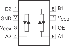
 Figure 4-1 DCT Or DCU Package8-Pin VSSOPTop View
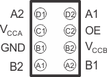
 Figure 4-2 YZP Package8-Pin DSBGABottom View
A. Pullup resistors are not
recommended on TXB0102 I/O pins.
B. If pullup resistors are needed
for open drain communication, please refer to the TXS0102 or contact TI.
C. If pullup or pulldown resistors
are needed, the resistor value must be over 50 kΩ. See Effects of External
Pullup and Pulldown Resistors on TXS and TXB Devices .
D. 50 kΩ is a safe recommended value,
if the customer can accept higher Vol or lower VCCOUT, smaller pullup
or pulldown resistor is allowed, the draft estimation is VOL =
VCCOUT × 4.5k/(4.5k + Rpu) and VOH = VCCOUT
× Rdw/(4.5k + Rdw).
E. For detailed information, See
A Guide to Voltage Translation With TXB-Type
Translators.
Table 4-1 Pin Functions: YZP
| PIN | TYPE(1) | DESCRIPTION | |
|---|---|---|---|
| NO. | NAME | ||
| A1 | B2 | I/O | Input/output B2. Referenced to VCCB. |
| A2 | B1 | I/O | Input/output B1. Referenced to VCCB. |
| B1 | GND | S | Ground |
| B2 | VCCB | S | B-port supply voltage. 1.65 V ≤ VCCB ≤ 5.5 V |
| C1 | VCCA | S | A-port supply voltage. 1.1 V ≤ VCCA ≤ 3.6 V, VCCA ≤ VCCB |
| C2 | OE | I | 3-state output-mode enable. Pull OE low to place all outputs in 3-state mode. Referenced to VCCA |
| D1 | A2 | I/O | Input/output A2. Referenced to VCCA |
| D2 | A1 | I/O | Input/output A1. Referenced to VCCA |
(1) I = input, O = output, I/O = input and output, S = power
supply
Table 4-2 Pin Functions: DCT or
DCU
| PIN | TYPE(1) | DESCRIPTION | |
|---|---|---|---|
| NAME | NO. | ||
| B2 | 1 | I/O | Input/output B2. Referenced to VCCB |
| GND | 2 | S | Ground |
| VCCA | 3 | S | A-port supply voltage. 1.1 V ≤ VCCA ≤ 3.6 V, VCCA ≤ VCCB |
| A2 | 4 | I/O | Input/output A2. Referenced to VCCA |
| A1 | 5 | I/O | Input/output A1. Referenced to VCCA |
| OE | 6 | I | 3-state output-mode enable. Pull OE low to place all outputs in 3-state mode. Referenced to VCCA |
| VCCB | 7 | S | B-port supply voltage. 1.65 V ≤ VCCB ≤ 5.5 V |
| B1 | 8 | I/O | Input/output B1. Referenced to VCCB |
(1) I = input, O = output, I/O = input and output, S = power
supply