SCES640J january 2007 – july 2023 TXS0102
PRODUCTION DATA
- 1
- 1 Features
- 2 Applications
- 3 Description
- 4 Revision History
- 5 Pin Configuration and Functions
-
6 Specifications
- 6.1 Absolute Maximum Ratings
- 6.2 ESD Ratings
- 6.3 Recommended Operating Conditions
- 6.4 Thermal Information
- 6.5 Electrical Characteristics
- 6.6 Timing Requirements: VCCA = 1.8 V ±0.15 V
- 6.7 Timing Requirements: VCCA = 2.5 V ± 0.2 V
- 6.8 Timing Requirements: VCCA = 3.3 V ± 0.3 V
- 6.9 Switching Characteristics: VCCA = 1.8 V ± 0.15 V
- 6.10 Switching Characteristics: VCCA = 2.5 V ± 0.2 V
- 6.11 Switching Characteristics: VCCA = 3.3 V ± 0.3 V
- 6.12 Typical Characteristics
- 7 Parameter Measurement Information
- 8 Detailed Description
- 9 Application and Implementation
- 10Device and Documentation Support
- 11Mechanical, Packaging, and Orderable Information
Package Options
Mechanical Data (Package|Pins)
Thermal pad, mechanical data (Package|Pins)
- DQM|8
Orderable Information
3 Description
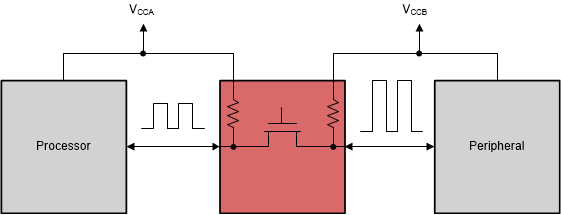
This two-bit non-inverting translator is a bidirectional voltage-level translator and can be used to establish digital switching compatibility between mixed-voltage systems. It uses two separate configurable power-supply rails, with the A ports supporting operating voltages from 1.65 V to 3.6 V while it tracks the VCCA supply, and the B ports supporting operating voltages from 2.3 V to 5.5 V while it tracks the VCCB supply. This allows the support of both lower and higher logic signal levels while providing bidirectional translation capabilities between any of the 1.8-V, 2.5-V, 3.3-V, and 5-V voltage nodes.
When the output-enable (OE) input is low, all I/Os are placed in the high-impedance state, which significantly reduces the power-supply quiescent current consumption.
To ensure the high-impedance state during power up or power down, OE should be tied to GND through a pulldown resistor; the minimum value of the resistor is determined by the current-sourcing capability of the driver.
| PART NUMBER | PACKAGE(1) | BODY SIZE (NOM) |
|---|---|---|
| TXS0102 | DCT (SSOP, 8) | 2.95 mm × 2.80 mm |
| DCU (VSSOP, 8) | 2.30 mm × 2.00 mm | |
| DQE (X2SON, 8) | 1.40 mm × 1.00 mm | |
| DQM (X2SON, 8) | 1.80 mm × 1.20 mm | |
| YZP (DSBGA, 8) | 1.90 mm × 0.90 mm |
 Typical Application Block Diagram for TXS0102