SCES642K December 2007 – April 2024 TXS0108E
PRODUCTION DATA
- 1
- 1 Features
- 2 Applications
- 3 Description
- 4 Pin Configuration and Functions
-
5 Specifications
- 5.1 Absolute Maximum Ratings
- 5.2 ESD Ratings
- 5.3 Recommended Operating Conditions
- 5.4 Thermal Information
- 5.5 Electrical Characteristics: TA = –40°C to 85°C
- 5.6 Timing Requirements: VCCA = 1.5V ± 0.1 V
- 5.7 Timing Requirements: VCCA = 1.8V ± 0.15V
- 5.8 Timing Requirements: VCCA = 2.5V ± 0.2V
- 5.9 Timing Requirements: VCCA = 3.3V ± 0.3V
- 5.10 Switching Characteristics: VCCA = 1.5V ± 0.1V
- 5.11 Switching Characteristics: VCCA = 1.8V ± 0.15V
- 5.12 Switching Characteristics: VCCA = 2.5V ± 0.2V
- 5.13 Switching Characteristics: VCCA = 3.3V ± 0.3V
- 5.14 Operating Characteristics: VCCA = 1.5V to 3.3V, VCCB = 1.5V to 3.3V
- 5.15 Typical Characteristics
- 6 Parameter Measurement Information
- 7 Detailed Description
- 8 Application and Implementation
- 9 Device and Documentation Support
- 10Revision History
- 11Mechanical, Packaging, and Orderable Information
Package Options
Mechanical Data (Package|Pins)
Thermal pad, mechanical data (Package|Pins)
- RGY|20
Orderable Information
3 Description
This device is an 8-bit non-inverting level translator which uses two separate configurable power-supply rails. The A port tracks the VCCA pin supply voltage. The VCCA pin accepts any supply voltage between 1.4V and 3.6V. The B port tracks the VCCB pin supply voltage. The VCCB pin accepts any supply voltage between 1.65V and 5.5V. Two input supply pins allows for low Voltage bidirectional translation between any of the 1.5V, 1.8V, 2.5V, 3.3V, and 5V voltage nodes.
When the output-enable (OE) input is low, all outputs are placed in the high-impedance (Hi-Z) state.
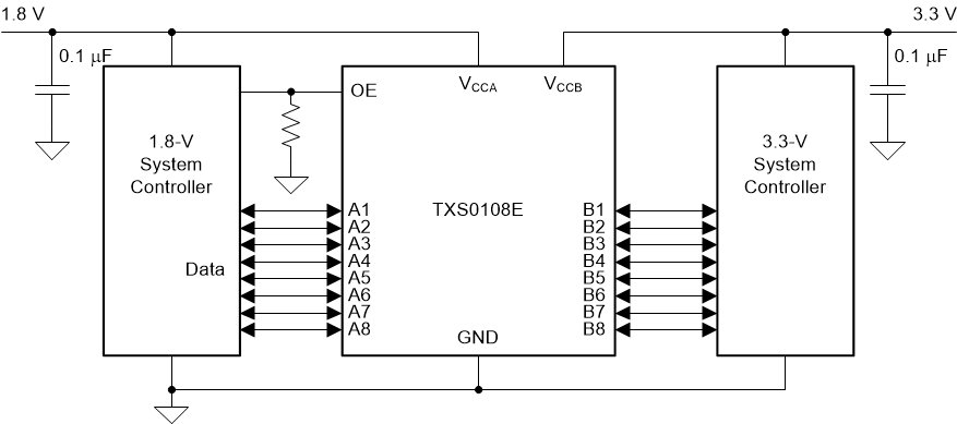
To put the device in the Hi-Z state during power-up or power-down periods, tie OE to GND through a pull-down resistor. The current-sourcing capability of the driver determines the minimum value of the resistor.
| PART NUMBER | PACKAGE(1) | PACKAGE SIZE(2) |
|---|---|---|
| TXS0108E | PW (TSSOP, 20) | 6.50mm × 6.40mm |
| RGY (VQFN, 20) | 4.50mm × 3.50mm | |
| ZXY (UFBGA, 20) | 2.50mm × 3.00mm | |
| NME (NFBGA, 20) | 2.50mm × 3.00mm |
 Simplified Application