SLUS557G March   2003  – December 2016 UC28023 , UC28025

PRODUCTION DATA.  

  1. Features
  2. Applications
  3. Description
  4. Revision History
  5. Pin Configuration and Functions
  6. Specifications
    1. 6.1 Absolute Maximum Ratings
    2. 6.2 ESD Ratings
    3. 6.3 Recommended Operating Conditions
    4. 6.4 Thermal Information
    5. 6.5 Electrical Characteristics
    6. 6.6 Switching Characteristics
    7. 6.7 Typical Characteristics
  7. Parameter Measurement Information
    1. 7.1 Control Methods and Test Circuits
  8. Detailed Description
    1. 8.1 Overview
    2. 8.2 Functional Block Diagram
    3. 8.3 Feature Description
      1. 8.3.1 Error Amplifier
      2. 8.3.2 Synchronization
      3. 8.3.3 Constant Volt-Second Clamp Circuit
      4. 8.3.4 Outputs
      5. 8.3.5 Open-Loop Laboratory Test Fixture
    4. 8.4 Device Functional Modes
  9. Application and Implementation
    1. 9.1 Application Information
    2. 9.2 Typical Application
      1. 9.2.1 Design Requirements
      2. 9.2.2 Detailed Design Procedure
        1. 9.2.2.1 Timing Resistor and Capacitor Selection
        2. 9.2.2.2 Turns Ratio Selection
        3. 9.2.2.3 Inductor Selection
        4. 9.2.2.4 Rectifier Diode Selection
        5. 9.2.2.5 Snubber Components Selection
        6. 9.2.2.6 VCC and VC Capacitor Selection
        7. 9.2.2.7 Output Capacitor Selection
        8. 9.2.2.8 Input Capacitor Selection
      3. 9.2.3 Application Curves
  10. 10Power Supply Recommendations
  11. 11Layout
    1. 11.1 Layout Guidelines
    2. 11.2 Layout Example
  12. 12Device and Documentation Support
    1. 12.1 Documentation Support
      1. 12.1.1 Related Documentation
    2. 12.2 Related Links
    3. 12.3 Receiving Notification of Documentation Updates
    4. 12.4 Community Resources
    5. 12.5 Trademarks
    6. 12.6 Electrostatic Discharge Caution
    7. 12.7 Glossary
  13. 13Mechanical, Packaging, and Orderable Information

Package Options

Refer to the PDF data sheet for device specific package drawings

Mechanical Data (Package|Pins)
  • DW|16
  • N|16
Thermal pad, mechanical data (Package|Pins)
Orderable Information

Parameter Measurement Information

Control Methods and Test Circuits

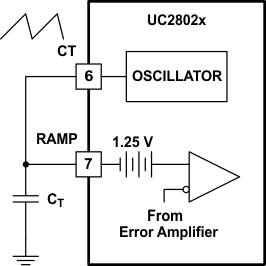
UC28023 UC28025 voltage_mode_control_slus557.gif Figure 7. Voltage Mode Control
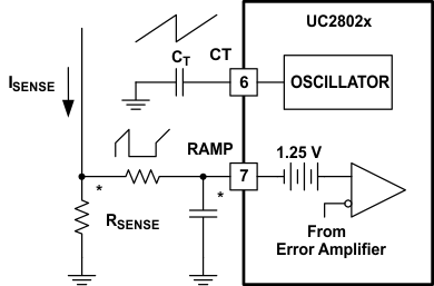
UC28023 UC28025 peak_current_mode_control_slus557.gif
A small filter may be required to suppress switch noise.
Figure 8. Peak Current Mode Control
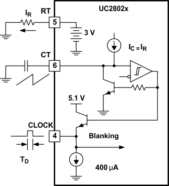
UC28023 UC28025 oscillator_circuit_slus557.gif Figure 9. Oscillator Circuit
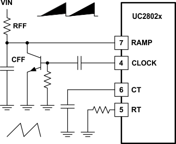
UC28023 UC28025 feedforward_technique_off_line_slus557.gif Figure 10. Feedforward Technique for Off-Line Voltage-Mode Applications