SLUS334F August 1995 – August 2022 UC1823A , UC1825A , UC2823A , UC2823B , UC2825A , UC2825B , UC3823A , UC3823B , UC3825A , UC3825B
PRODUCTION DATA
- 1Features
- 2Description
- 3Revision History
- 4Ordering Information
- 5Pin Configuration and Functions
- 6Specifications
- 7Application and Implementation
- 8Device and Documentation Support
- 9Mechanical, Packaging, and Orderable Information
Package Options
Refer to the PDF data sheet for device specific package drawings
Mechanical Data (Package|Pins)
- DW|16
Thermal pad, mechanical data (Package|Pins)
Orderable Information
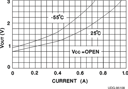
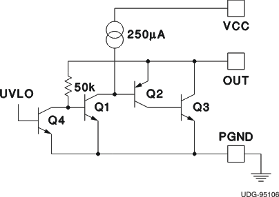
7.3 ACTIVE LOW OUTPUTS DURING UVLO
The UVLO function forces the outputs to be low and considers both VCC and VREF before allowing the chip to operate.
 Figure 7-3 Output Voltage vs Output Current
 Figure 7-4 Output V and I During UVLO