SLUSCZ8 July 2017 UCC27212A-Q1
PRODUCTION DATA.
- 1 Features
- 2 Applications
- 3 Description
- 4 Revision History
- 5 Pin Configuration and Functions
- 6 Specifications
- 7 Detailed Description
- 8 Application and Implementation
- 9 Power Supply Recommendations
- 10Layout
- 11Device and Documentation Support
- 12Mechanical, Packaging, and Orderable Information
Package Options
Mechanical Data (Package|Pins)
- DDA|8
Thermal pad, mechanical data (Package|Pins)
- DDA|8
Orderable Information
7 Detailed Description
7.1 Overview
The UCC27212A-Q1 device represents Texas Instruments’ latest generation of high-voltage gate drivers, which are designed to drive both the high-side and low-side of N-Channel MOSFETs in a half- and full-bridge or synchronous-buck configuration. The floating high-side driver can operate with supply voltages of up to 120 V, which allows for N-Channel MOSFET control in half-bridge, full-bridge, push-pull, two-switch forward, and active clamp forward converters.
The UCC27212A-Q1 device feature 4-A source and sink capability, industry best-in-class switching characteristics and a host of other features listed in Table 1. These features combine to ensure efficient, robust and reliable operation in high-frequency switching power circuits.
Table 1. UCC27212A-Q1 Highlights
| FEATURE | BENEFIT |
|---|---|
| 4-A source and sink current with 0.9-Ω output resistance | High peak current ideal for driving large power MOSFETs with minimal power loss (fast-drive capability at Miller plateau) |
| Input pins (HI and LI) can directly handle –10 VDC up to 20 VDC | Increased robustness and ability to handle undershoot and overshoot can interface directly to gate-drive transformers without having to use rectification diodes. |
| 120-V internal boot diode | Provides voltage margin to meet telecom 100-V surge requirements |
| Switch node (HS pin) able to handle –18 V maximum for 100 ns | Allows the high-side channel to have extra protection from inherent negative voltages caused by parasitic inductance and stray capacitance |
| Robust ESD circuitry to handle voltage spikes | Excellent immunity to large dV/dT conditions |
| 18-ns propagation delay with 7.2-ns rise time and 5.5-ns fall time | Best-in-class switching characteristics and extremely low-pulse transmission distortion |
| 2-ns (typical) delay matching between channels | Avoids transformer volt-second offset in bridge |
| Symmetrical UVLO circuit | Ensures high-side and low-side shut down at the same time |
| TTL optimized thresholds with increased hysteresis | Complementary to analog or digital PWM controllers; increased hysteresis offers added noise immunity |
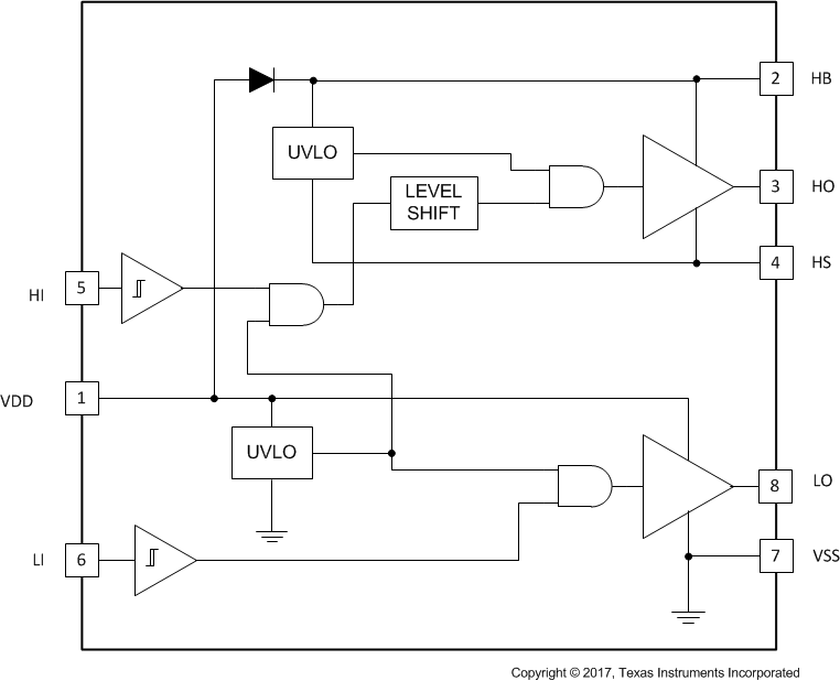
In the UCC27212A-Q1 device, the high side and low side each have independent inputs that allow maximum flexibility of input control signals in the application. The boot diode for the high-side driver bias supply is internal to the UCC27212A-Q1. The UCC27212A-Q1 is the TTL or logic compatible version. The high-side driver is referenced to the switch node (HS), which is typically the source pin of the high-side MOSFET and drain pin of the low-side MOSFET. The low-side driver is referenced to VSS, which is typically ground. The UCC27212A-Q1 functions are divided into the input stages, UVLO protection, level shift, boot diode, and output driver stages.
7.2 Functional Block Diagram

7.3 Feature Description
7.3.1 Input Stages
The input stages provide the interface to the PWM output signals. The input stages of the UCC27212A-Q1 device have impedance of 70-kΩ nominal and input capacitance is approximately 2 pF. Pulldown resistance to VSS (ground) is 70 kΩ. The logic level compatible input provides a rising threshold of 2.3 V and a falling threshold of 1.6 V. There is enough input hysteresis to avoid noise related jitter issues on the input.
7.3.2 Undervoltage Lockout (UVLO)
The bias supplies for the high-side and low-side drivers have UVLO protection. VDD as well as VHB to VHS differential voltages are monitored. The VDD UVLO disables both drivers when VDD is below the specified threshold. The rising VDD threshold is 5.7 V with 0.4-V hysteresis. The VHB UVLO disables only the high-side driver when the VHB to VHS differential voltage is below the specified threshold. The VHB UVLO rising threshold is 5.3 V with 0.4 V hysteresis.
7.3.3 Level Shift
The level shift circuit is the interface from the high-side input to the high-side driver stage which is referenced to the switch node (HS). The level shift allows control of the HO output referenced to the HS pin and provides excellent delay matching with the low-side driver.
7.3.4 Boot Diode
The boot diode necessary to generate the high-side bias is included in the UCC27212A-Q1 family of drivers. The diode anode is connected to VDD and cathode connected to VHB. With the VHB capacitor connected to HB and the HS pins, the VHB capacitor charge is refreshed every switching cycle when HS transitions to ground. The boot diode provides fast recovery times, low diode resistance, and voltage rating margin to allow for efficient and reliable operation.
7.3.5 Output Stages
The output stages are the interface to the power MOSFETs in the power train. High slew rate, low resistance and high peak current capability of both output drivers allow for efficient switching of the power MOSFETs. The low-side output stage is referenced from VDD to VSS and the high side is referenced from VHB to VHS.
7.4 Device Functional Modes
The device operates in normal mode and UVLO mode. See the Undervoltage Lockout (UVLO) section for information on UVLO operation mode. In the normal mode the output state is dependent on states of the HI and LI pins. Table 2 lists the output states for different input pin combinations.