SLUS504I September 2002 – November 2023 UCC27321 , UCC27322 , UCC37321 , UCC37322
PRODUCTION DATA
- 1
- 1 Features
- 2 Applications
- 3 Description
- 4 Description (continued)
- 5 Related Products
- 6 Pin Configuration and Functions
- 7 Specifications
- 8 Detailed Description
- 9 Application and Implementation
- 10Power Supply Recommendations
- 11Layout
- 12Device and Documentation Support
- 13Revision History
- 14Mechanical, Packaging, and Orderable Information
Package Options
Refer to the PDF data sheet for device specific package drawings
Mechanical Data (Package|Pins)
- D|8
- P|8
- DGN|8
Thermal pad, mechanical data (Package|Pins)
- DGN|8
Orderable Information
7.7 Power Dissipation Ratings
| PACKAGE | SUFFIX | θjc (°C/W) | θja (°C/W) | Power Rating (mW) TA = 70°C(1) | Derating Factor Above 70°C (mW/°C)(1) |
|---|---|---|---|---|---|
| SOIC-8 | D | 42 | 84 to 160(2) | 344 to 655(2) | 6.25 to 11.9(2) |
| MSOP PowerPAD-8 | DGN | 4.7 | 50 to 59 | 1370 | 17.1 |
(1) 125°C operating junction temperature is used for power rating calculations
(2) The range of values indicates the effect of the printed-circuit-board. These values are intended to give the system designer an indication of the best and worst case conditions. In general, the system designer should attempt to use larger traces on the printed-circuit-board where possible to spread the heat away form the device more effectively. For additional information on device temperature management, see the Packaging Information section of the Power Supply Control Products Data Book, (SLUD003).

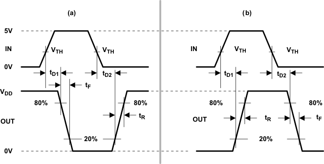
The 20% and 80% thresholds depict the dynamics of the BiPolar output devices that dominate the power MOSFET transition through the Miller regions of operation.
Figure 7-1 Switching Waveforms for (a) Inverting Input to (b) Output Times
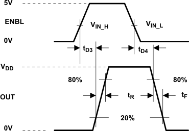
The 20% and 80% thresholds depict the dynamics of the BiPolar output devices that dominate the power MOSFET transition through the Miller regions of operation.
Figure 7-2 Switching Waveform for Enable to Output