SLUS504I September 2002 – November 2023 UCC27321 , UCC27322 , UCC37321 , UCC37322
PRODUCTION DATA
- 1
- 1 Features
- 2 Applications
- 3 Description
- 4 Description (continued)
- 5 Related Products
- 6 Pin Configuration and Functions
- 7 Specifications
- 8 Detailed Description
- 9 Application and Implementation
- 10Power Supply Recommendations
- 11Layout
- 12Device and Documentation Support
- 13Revision History
- 14Mechanical, Packaging, and Orderable Information
Package Options
Refer to the PDF data sheet for device specific package drawings
Mechanical Data (Package|Pins)
- D|8
- P|8
- DGN|8
Thermal pad, mechanical data (Package|Pins)
- DGN|8
Orderable Information
6 Pin Configuration and Functions
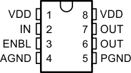
 Figure 6-1
D, and DGN Packages8-Pin SOIC, and MSOP
With PowerPADTop View
Figure 6-1
D, and DGN Packages8-Pin SOIC, and MSOP
With PowerPADTop ViewTable 6-1 Pin Functions
| PIN | I/O | DESCRIPTION | |
|---|---|---|---|
| NAME | NO. | ||
| AGND | 4 | — | The AGND and the PGND must be connected by a single thick trace directly under the device. There must be a low ESR, low ESL capacitor of 0.1 µF between VDD (pin 8) and PGND and a separate 0.1-µF capacitor between VDD (pin 1) and AGND. The power MOSFETs must be located on the PGND side of the device while the control circuit must be on the AGND side of the device. The control circuit ground must be common with the AGND while the PGND must be common with the source of the power FETs. |
| ENBL | 3 | I | Enable input for the driver with logic compatible threshold and hysteresis. The driver output can be enabled and disabled with this pin. It is internally pulled up to VDD with 100-kΩ resistor for active high operation. When the device is disabled, the output state is, low regardless of the input state. |
| IN | 2 | I | Input signal of the driver which has logic compatible threshold and hysteresis. |
| OUT | 6, 7 | O | Driver outputs that must be connected together externally. The output stage is capable of providing 9-A peak drive current to the gate of a power MOSFET. |
| PGND | 5 | — | Common ground for output stage. This ground must be connected very closely to the source of the power MOSFET which the driver is driving. Grounds are separated to minimize ringing affects due to output switching di/dt which can affect the input threshold. |
| VDD | 1, 8 | I | Supply voltage and the power input connections for this device. Two pins must be connected together externally. |