SGLS274I September 2008 – November 2023 UCC27423-Q1 , UCC27424-Q1 , UCC27425-Q1
PRODUCTION DATA
- 1
- 1 Features
- 2 Applications
- 3 Description
- 4 Device Comparison Table
- 5 Pin Configuration and Functions
- 6 Specifications
- 7 Detailed Description
- 8 Application and Implementation
- 9 Power Supply Recommendations
- 10Layout
- 11Device and Documentation Support
- 12Revision History
- 13Mechanical, Packaging, and Orderable Information
Package Options
Mechanical Data (Package|Pins)
Thermal pad, mechanical data (Package|Pins)
- DGN|8
Orderable Information
3 Description
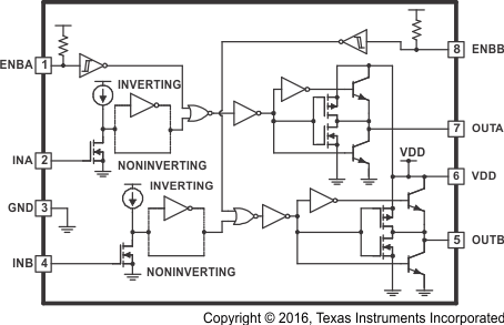
The UCC2742x-Q1 family of devices are high-speed dual MOSFET drivers capable of delivering large peak currents into capacitive loads. Two standard logic options are offered: dual inverting and dual noninverting drivers. They are offered in the standard 8-pin SOIC (D) package. The thermally enhanced 8-pin PowerPAD Package MSOP package (DGN) drastically lowers the thermal resistance to improve long-term reliability.
Using a design that inherently minimizes shoot-through current, these drivers deliver 4-A current where it is needed most, at the Miller plateau region, during the MOSFET switching transition. A unique bipolar and MOSFET hybrid output stage in parallel also allows efficient current sourcing and sinking at low supply voltages.
The UCC2742x-Q1 provide enable (ENBL) functions to have better control of the operation of the driver applications. ENBA and ENBB are implemented on pins 1 and 8, which were previously left unused in the industry standard pinout. They are internally pulled up to VDD for active-high logic and can be left open for standard operation.
| PART NUMBER(1) | PACKAGE | BODY SIZE (NOM) |
|---|---|---|
| UCC2742x-Q1 | SOIC (8) | 4.90 mm × 3.91 mm |
| MSOP With PowerPAD (8) | 3.00 mm × 3.00 mm |
 Block Diagram