SLVSC82B August 2013 – October 2015 UCC27531-Q1
PRODUCTION DATA.
- 1 Features
- 2 Applications
- 3 Description
- 4 Revision History
- 5 Description (continued)
- 6 Pin Configuration and Functions
- 7 Specifications
- 8 Detailed Description
- 9 Application and Implementation
- 10Power Supply Recommendations
- 11Layout
- 12Device and Documentation Support
- 13Mechanical, Packaging, and Orderable Information
Package Options
Mechanical Data (Package|Pins)
- DBV|6
Thermal pad, mechanical data (Package|Pins)
Orderable Information
1 Features
- Qualified for Automotive Applications
- AEC-Q100 Qualified with the Following Results:
- Device Temperature Grade 1
- Device HBM ESD Classification Level H2
- Device CDM ESD Classification Level C4B
- Low Cost Gate Driver (Offering Optimal Solution for Driving Fet And Igbts)
- Superior Replacement to Discrete Transistor Pair Drive (Providing Easy Interface With Controller)
- TTL and CMOS Compatible Input Logic Threshold, (Independent of Supply Voltage)
- Split Output Options Allow for Tuning of Turn-On and Turn-Off Currents
- Enable with Fixed TTL Compatible Threshold
- High 2.5-A Source and 5-A Sink Peak Drive Currents at 18-V VDD
- Wide VDD Range From 10 V up to 35 V
- Input and Enable Pins Capable of Withstanding up to –5-V DC Below Ground
- Output Held Low When Inputs are Floating or During VDD UVLO
- Fast Propagation Delays (17-ns Typical)
- Fast Rise and Fall Times
(15-ns and 7-ns Typical With 1800-pF Load) - Undervoltage Lockout (UVLO)
- Used as a High-Side or Low-Side Driver (if Designed With Proper Bias and Signal Isolation)
- Low-Cost, Space-Saving 6-Pin DBV (SOT-23) Package Options
- Operating Temperature Range of –40°C to 140°C
2 Applications
- Automotive
- Switch-Mode Power Supplies
- DC-to-DC Converters
- Solar Inverters, Motor Control, UPS
- HEV and EV Chargers
- Home Appliances
- Renewable Energy Power Conversion
- SiC FET Converters
3 Description
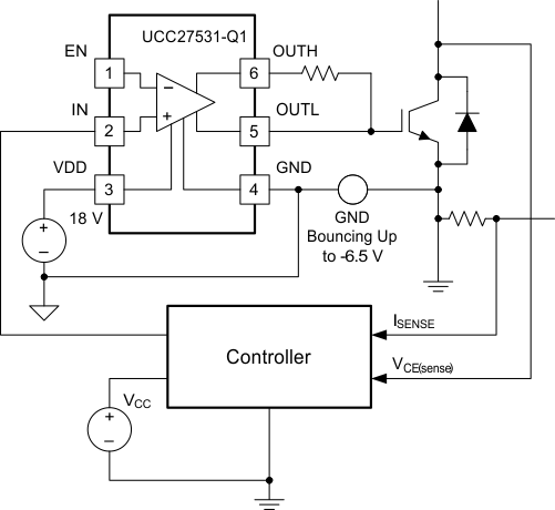
The UCC27531-Q1 is a single-channel, high-speed, gate driver capable of effectively driving MOSFET and IGBT power switches by using up to 2.5-A source and 5-A sink (asymmetrical drive) peak current. Strong sink capability in asymmetrical drive boosts immunity against parasitic Miller turn-on effect. The UCC27531-Q1 device can also feature a split-output configuration where the gate-drive current is sourced through the OUTH pin and sunk through the OUTL pin. This pin arrangement allows the user to apply independent turn-on and turn-off resistors to the OUTH and OUTL pins respectively and easily control the switching slew rates.
The driver has rail-to-rail drive capability and an extremely small propagation delay of typically 17 ns.
The input threshold of UCC27531-Q1 is based on TTL and CMOS compatible low-voltage logic, which is fixed and independent of VDD supply voltage. The 1-V typical hysteresis offers excellent noise immunity.
Device Information(1)
| PART NUMBER | PACKAGE | BODY SIZE (NOM) |
|---|---|---|
| UCC27531-Q1 | SOT-23 (6) | 1.6 mm × 2.9 mm |
- For all available packages, see the orderable addendum at the end of the data sheet.
Driving IGBT Without Negative Bias
