SLUSA12G December 2009 – November 2022 UCC28C40-Q1 , UCC28C41-Q1 , UCC28C42-Q1 , UCC28C43-Q1 , UCC28C44-Q1 , UCC28C45-Q1
PRODUCTION DATA
- 1 Features
- 2 Applications
- 3 Description
- 4 Revision History
- 5 Device Comparison Table
- 6 Pin Configuration and Functions
- 7 Specifications
-
8 Detailed Description
- 8.1 Overview
- 8.2 Functional Block Diagram
- 8.3 Feature Description
- 8.4 Device Functional Modes
-
9 Application and Implementation
- 9.1 Application Information
- 9.2
Typical Application
- 9.2.1 Design Requirements
- 9.2.2
Detailed Design Procedure
- 9.2.2.1 Custom Design With WEBENCH® Tools
- 9.2.2.2 Input Bulk Capacitor and Minimum Bulk Voltage
- 9.2.2.3 Transformer Turns Ratio and Maximum Duty CycleG
- 9.2.2.4 Transformer Inductance and Peak Currents
- 9.2.2.5 Output Capacitor
- 9.2.2.6 Current Sensing Network
- 9.2.2.7 Gate Drive Resistor
- 9.2.2.8 VREF Capacitor
- 9.2.2.9 RT/CT
- 9.2.2.10 Start-Up Circuit
- 9.2.2.11 Voltage Feedback Compensation
- 9.2.3 Application Curves
- 9.2.4 Power Supply Recommendations
- 9.2.5 Layout
- 10Device and Documentation Support
- 11Mechanical, Packaging, and Orderable Information
Package Options
Mechanical Data (Package|Pins)
- D|8
Thermal pad, mechanical data (Package|Pins)
Orderable Information
8.3.5 Reduced-Discharge Current Variation
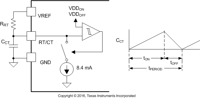
The UCC28C4x-Q1 oscillator design incorporates a trimmed discharge current to accurately program maximum duty cycle and operating frequency. In its basic operation, a timing capacitor (CCT) is charged by a current source, formed by the timing resistor (RRT) connected to the device’s reference voltage (VREF). The oscillator design incorporates comparators to monitor the amplitude of the timing capacitor’s voltage. The exponentially shaped waveform charges up to a specific amplitude representing the oscillator’s upper threshold of 2.5 V. Once reached, an internal current sink to ground is turned on and the capacitor begins discharging. This discharge continues until the oscillator’s lower threshold has reached 0.7 V at which point the current sink is turned off. Next, the timing capacitor starts charging again and a new switching cycle begins.
 Figure 8-4 Oscillator Circuit
While the device is discharging the timing capacitor, resistor RRT is also still trying to charge CCT. It is the exact ratio of these two currents, the discharging versus the charging current, which specifies the maximum duty cycle. During the discharge time of CCT, the device’s output is always off. This represents an ensured minimum off time of the switch, commonly referred to as dead-time. To program an accurate maximum duty cycle, use the information provided in Figure 7-15 for maximum duty cycle versus oscillator frequency. Any number of maximum duty cycles can be programmed for a given frequency by adjusting the values of RRT and CCT. Once RRT is selected, the oscillator timing capacitor can be found using the curves in Figure 7-1. However, because resistors are available in more precise increments, typically 1%, and capacitors are only available in 5% accuracy, it might be more practical to select the closest capacitor value first and then calculate the timing resistor value next.