SLUS495J August 2001 – December 2023 UCC29002 , UCC39002
PRODUCTION DATA
- 1
- 1Features
- 2Applications
- 3Description
- 4Pin Configuration and Functions
- 5Specifications
-
6Detailed Description
- 6.1 Overview
- 6.2 Functional Block Diagram
- 6.3
Feature Description
- 6.3.1 Differential Current-Sense Amplifier (CS+, CS−, CSO)
- 6.3.2 Load-Share Bus Driver Amplifier (CSO, LS)
- 6.3.3 Load-Share Bus Receiver Amplifier (LS)
- 6.3.4 Error Amplifier (EAO)
- 6.3.5 Adjust Amplifier Output (ADJ)
- 6.3.6 Enable Function (CS+, CS−)
- 6.3.7 Fault Protection on LS Bus
- 6.3.8 Start-Up and Adjust Logic
- 6.3.9 Bias Input and Bias_OK Circuit (VDD)
- 6.4 Device Functional Modes
- 7Application and Implementation
- 8Device and Documentation Support
- 9Revision History
- Mechanical, Packaging, and Orderable Information
Package Options
Mechanical Data (Package|Pins)
Thermal pad, mechanical data (Package|Pins)
- DGK|8
Orderable Information
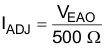
6.3.5 Adjust Amplifier Output (ADJ)
A feedback-loop adjustment current IADJ, proportional to the error voltage VEAO on pin 6, is sunk by the ADJ pin. This current flows through the parallel combination of the module's remote-sense resistor RSENSE and the adjust resistor, RADJ. The effect of IADJ is to increase the output voltage of the module influenced by the UCC29002 device. The amplitude of IADJ is set by the 500Ω internal resistor between the emitter of the amplifier's open-collector output transistor and ground shown in the Functional Block Diagram. Use Equation 2 to calculate the magnitude of IADJ. Maximum IADJ occurs at maximum VEAO.
At the leader module, VEAO is 0V and consequently the adjust current must be zero as well. Therefore, the output voltage of the leader module remains at its initial output voltage set point at all times.
During the start-up mode of the UCC29002, the noninverting input of the Adjust amplifier is switched to 3V to increase the module's output voltage significantly and quickly match the starting module's output current to the other modules' currents.
In cases of insufficient VDD bias level, LS bus fault, or disabled UCC29002 (by CS+, CS- inputs), the noninverting input of the Adjust amplifier is switched to ground to prevent erroneous adjustment of the module's output voltage by the load-share controller.