SLUS495J August 2001 – December 2023 UCC29002 , UCC39002
PRODUCTION DATA
- 1
- 1Features
- 2Applications
- 3Description
- 4Pin Configuration and Functions
- 5Specifications
-
6Detailed Description
- 6.1 Overview
- 6.2 Functional Block Diagram
- 6.3
Feature Description
- 6.3.1 Differential Current-Sense Amplifier (CS+, CS−, CSO)
- 6.3.2 Load-Share Bus Driver Amplifier (CSO, LS)
- 6.3.3 Load-Share Bus Receiver Amplifier (LS)
- 6.3.4 Error Amplifier (EAO)
- 6.3.5 Adjust Amplifier Output (ADJ)
- 6.3.6 Enable Function (CS+, CS−)
- 6.3.7 Fault Protection on LS Bus
- 6.3.8 Start-Up and Adjust Logic
- 6.3.9 Bias Input and Bias_OK Circuit (VDD)
- 6.4 Device Functional Modes
- 7Application and Implementation
- 8Device and Documentation Support
- 9Revision History
- Mechanical, Packaging, and Orderable Information
Package Options
Mechanical Data (Package|Pins)
Thermal pad, mechanical data (Package|Pins)
- DGK|8
Orderable Information
3 Description
The UCC29002 device family comprises advanced, high-performance, low-cost load-share controllers that provide all necessary functions to parallel multiple independent power supplies or DC-to-DC modules. Targeted for high-reliability applications in server, workstation, telecom, and other distributed power systems, the controller is suitable for N+1 redundant systems or high-current applications where off-the-shelf power supplies must be paralleled.
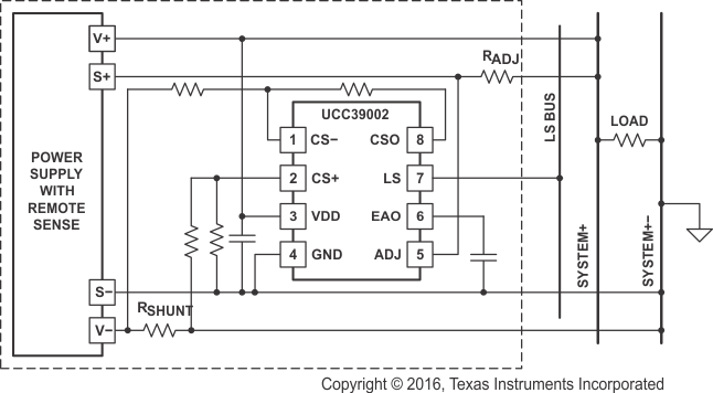
The BiCMOS UCC29002 is based on the automatic leader/follower architecture of predecessor UC3902 and UC3907 load-share controllers. The device is capable of better than 1% current-share error between modules at full load by using a very-low offset post-package-trimmed current-sense amplifier and a high-gain negative-feedback loop. With an amplifier common-mode range of 0V to the VDD supply rail, the current-sense resistor, RSHUNT, can be placed in either the GND return path or in the positive output rail of the power supply.
| PART NUMBER | PACKAGE(1) | PACKAGE SIZE (NOM)(2) |
|---|---|---|
| UCC29002 UCC29002-1(3) UCC39002 | SOIC (8) | 4.90mm × 6.00mm |
| UCC29002 UCC39002 | VSSOP (8) | 3.00mm × 4.90mm |
| PDIP (8) | 9.81mm × 9.43mm |
 Typical
Low-Side Current-Sensing Application