SLUS652E March   2005  – April 2020 UCD8220

PRODUCTION DATA.  

  1. Features
  2. Applications
  3. Description
    1. 3.1 UCD8220 Typical Simplified Push-Pull Converter Application Schematic
  4. Revision History
  5. Pin Configuration and Functions
    1.     Pin Functions
  6. Specifications
    1. 6.1 Absolute Maximum Ratings
    2. 6.2 ESD Ratings
    3. 6.3 Recommended Operating Conditions
    4. 6.4 Thermal Information
    5. 6.5 Electrical Characteristics
    6. 6.6 Timing Requirements
    7. 6.7 Typical Characteristics
  7. Detailed Description
    1. 7.1 Overview
    2. 7.2 Functional Block Diagram
    3. 7.3 Feature Description
      1. 7.3.1 CLK Input Time-Domain Digital Pulse Train
      2. 7.3.2 Current Sensing and Protection
      3. 7.3.3 Handshaking
      4. 7.3.4 Driver Output
      5. 7.3.5 Source and Sink Capabilities During Miller Plateau
      6. 7.3.6 Drive Current and Power Requirements
      7. 7.3.7 Clearing the Current-Limit Flag (CLF)
    4. 7.4 Device Functional Modes
  8. Application and Implementation
    1. 8.1 Application Information
    2. 8.2 Typical Application
      1. 8.2.1 Design Requirements
      2. 8.2.2 Detailed Design Procedure
        1. 8.2.2.1 Selecting the ISET Resistor for Voltage Mode Control
        2. 8.2.2.2 Selecting the ISET Resistor for Voltage Mode Control with Voltage Feed Forward
        3. 8.2.2.3 Selecting the ISET Resistor for Peak Current Mode Control with Internal Slope Compensation
      3. 8.2.3 Application Curves
  9. Power Supply Recommendations
  10. 10Layout
    1. 10.1 Layout Guidelines
    2. 10.2 Layout Example
    3. 10.3 Thermal Considerations
  11. 11Device and Documentation Support
    1. 11.1 Documentation Support
      1. 11.1.1 Related Documentation
    2. 11.2 Trademarks
    3. 11.3 Electrostatic Discharge Caution
    4. 11.4 Glossary
  12. 12Mechanical, Packaging, and Orderable Information

Package Options

Refer to the PDF data sheet for device specific package drawings

Mechanical Data (Package|Pins)
  • PWP|16
Thermal pad, mechanical data (Package|Pins)
Orderable Information

Application Curves

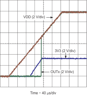
UCD8220 start_12v_3v3_slusb36.gif
CLK = CTRL = 3V3
Figure 36. Start-Up Behavior at VDD = 12 V
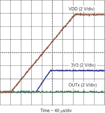
UCD8220 start_12v_gnd_slusb36.gif
CLK = AGND CTRL = 3V3
Figure 38. Start-Up Behavior at VDD = 12 V
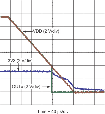
UCD8220 shut_12v_3v3_slusb36.gif
CLK = CTRL = 3V3
Figure 37. Shut-Down Behavior at VDD = 12 V
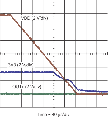
UCD8220 shut_12v_gnd_slusb36.gif
CLK = AGND CTRL = 3V3
Figure 39. Shut-Down Behavior at VDD = 12 V