SGLS148E December 2002 – December 2015 ULQ2003A-Q1 , ULQ2004A-Q1
PRODUCTION DATA.
- 1 Features
- 2 Applications
- 3 Description
- 4 Revision History
- 5 Pin Configuration and Functions
-
6 Specifications
- 6.1 Absolute Maximum Ratings
- 6.2 ESD Ratings
- 6.3 Recommended Operating Conditions
- 6.4 Thermal Information
- 6.5 Electrical Characteristics, ULQ2003AT and ULQ2003AQ
- 6.6 Electrical Characteristics, ULQ2004AT
- 6.7 Switching Characteristics, ULQ2003A and ULQ2004A
- 6.8 Dissipation Ratings
- 6.9 Typical Characteristics
- 7 Parameter Measurement Information
- 8 Detailed Description
- 9 Application and Implementation
- 10Power Supply Recommendations
- 11Layout
- 12Device and Documentation Support
- 13Mechanical, Packaging, and Orderable Information
Package Options
Refer to the PDF data sheet for device specific package drawings
Mechanical Data (Package|Pins)
- D|16
Thermal pad, mechanical data (Package|Pins)
- D|16
Orderable Information
7 Parameter Measurement Information
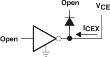 Figure 3. ICEX Test Circuit
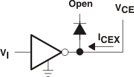 Figure 4. ICEX Test Circuit
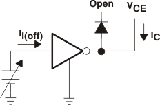 Figure 5. II(off) Test Circuit
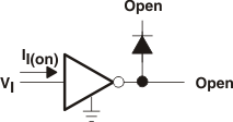 Figure 6. II Test Circuit
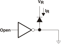 Figure 7. IR Test Circuit
 Figure 8. VF Test Circuit
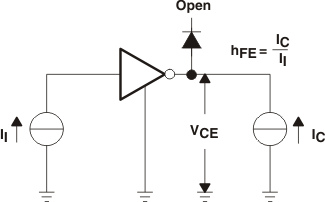
A. II is fixed for measuring VCE(sat), variable for measuring hFE.
Figure 9. hFE, VCE(sat) Test Circuit
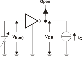 Figure 10. VI(on) Test Circuit
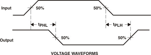 Figure 11. Propagation Delay-Time Waveforms
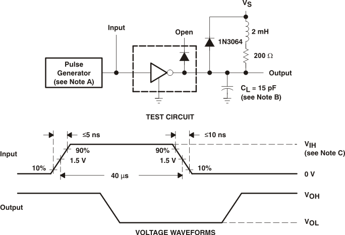
A. The pulse generator has the following characteristics: PRR = 12.5 kHz, ZO = 50 Ω.
B. CL includes probe and jig capacitance.
C. For testing the ULQ2003A, VIH = 3 V; for the ULQ2004A, VIH = 8 V.
Figure 12. Latch-Up Test Circuit and Voltage Waveforms