SLES275A January 2015 – December 2017 VSP5324-Q1
PRODUCTION DATA.
- 1 Features
- 2 Applications
- 3 Description
- 4 Revision History
- 5 Pin Configuration and Functions
-
6 Specifications
- 6.1 Absolute Maximum Ratings
- 6.2 ESD Ratings
- 6.3 Recommended Operating Conditions
- 6.4 Thermal Information
- 6.5 Electrical Characteristics: Dynamic Performance
- 6.6 Electrical Characteristics: General
- 6.7 Electrical Characteristics: Digital
- 6.8 Timing Requirements
- 6.9 LVDS Timing at Different Sampling Frequencies (One-Lane Interface, 12x Serialization)
- 6.10 LVDS Timing at Different Sampling Frequencies (Two-Lane Interface, 6x Serialization)
- 6.11 Serial Interface Timing Requirements
- 6.12 Typical Characteristics
-
7 Detailed Description
- 7.1 Overview
- 7.2 Functional Block Diagrams
- 7.3 Feature Description
- 7.4 Device Functional Modes
- 7.5 Programming
- 7.6
Register Maps
- 7.6.1
Serial Registers
- 7.6.1.1 Register 00h (offset = 00h) [reset = 0]
- 7.6.1.2 Register 01h (offset = 01h) [reset = 0]
- 7.6.1.3 Register 02h (offset = 02h) [reset = 0]
- 7.6.1.4 Register 0Ah (offset = 0Ah) [reset = 0]
- 7.6.1.5 Register 0Fh (offset = 0Fh) [reset = 0]
- 7.6.1.6 Register 14h (offset = 14h) [reset = 0]
- 7.6.1.7 Register 1Ch (offset = 1Ch) [reset = 0]
- 7.6.1.8 Register 23h (offset = 23h) [reset = 0]
- 7.6.1.9 Register 24h (offset = 24h) [reset = 0]
- 7.6.1.10 Register 25h (offset = 25h) [reset = 0]
- 7.6.1.11 Register 26h (offset = 26h) [reset = 0]
- 7.6.1.12 Register 27h (offset = 27h) [reset = 0]
- 7.6.1.13 Register 28h (offset = 28h) [reset = 0]
- 7.6.1.14 Register 29h (offset = 29h) [reset = 0]
- 7.6.1.15 Register 2Ah (offset = 2Ah) [reset = 0]
- 7.6.1.16 Register 2Bh (offset = 2Bh) [reset = 0]
- 7.6.1.17 Register 2Eh (offset = 2Eh) [reset = 0]
- 7.6.1.18 Register 30h (offset = 30h) [reset = 0]
- 7.6.1.19 Register 33h (offset = 33h) [reset = 0]
- 7.6.1.20 Register 35h (offset = 35h) [reset = 0]
- 7.6.1.21 Register 38h (offset = 38h) [reset = 0x0000]
- 7.6.1.22 Register 42h (offset = 42h) [reset = 0]
- 7.6.1.23 Register 45h (offset = 45h) [reset = 0]
- 7.6.1.24 Register 46h (offset = 46h) [reset = 0]
- 7.6.1.25 Register 50h (offset = 50h) [reset = 0]
- 7.6.1.26 Register 51h (offset = 51h) [reset = 0]
- 7.6.1.27 Register 53h (offset = 53h) [reset = 0]
- 7.6.1.28 Register 54h (offset = ) [reset = 0]
- 7.6.1.29 Register 55h (offset = 55h) [reset = 0]
- 7.6.1.30 Register F0h (offset = F0h) [reset = 0]
- 7.6.1
Serial Registers
- 8 Application and Implementation
- 9 Power Supply Recommendations
- 10Layout
- 11Device and Documentation Support
- 12Mechanical, Packaging, and Orderable Information
Package Options
Mechanical Data (Package|Pins)
- RGC|64
Thermal pad, mechanical data (Package|Pins)
- RGC|64
Orderable Information
8 Application and Implementation
NOTE
Information in the following applications sections is not part of the TI component specification, and TI does not warrant its accuracy or completeness. TI’s customers are responsible for determining suitability of components for their purposes. Customers should validate and test their design implementation to confirm system functionality.
8.1 Application Information
The VSP5324-Q1 device is a low power 12-bit, 4-channel ADC customized for time-of-flight applications. The device accepts four single-ended or differential analog inputs and can be configured to output the digitized data on 4 or 8 LVDS lanes as per the requirements of the external host receiver. The sampling clock can be fed to the device using a single-ended or a differential signal. High-speed sampling rates of up to 80 MSPS can be used to speed up the sensor readout and therefore use longer sensor exposure times without taking a hit on the frame-rate. The device is controlled using a simple 4-wire SPI. Power constrained systems can additionally make use of the power-down pin (PD) to take the device quickly in and out of low-power mode. The device uses an internal reference and internal common-mode voltage by default and has a provision for the use of external reference and external common-mode voltage inputs.
8.2 Typical Application
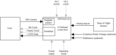 Figure 80. Application Schematic
8.2.1 Design Requirements
For optimum performance, the analog inputs must be driven differentially. If the inputs are driven in a single-ended manner, capacitors must be placed on the INx_M signals and close to the INx_M pins. An optional 5-Ω to 15-Ω resistor in series with each input pin can be kept to damp out ringing caused by package parasitics. The drive circuit may have to be designed to minimize the impact of kick-back noise generated by sampling switches opening and closing inside the ADC, as well as ensuring low insertion loss over the desired frequency range and matched impedance to the source.
8.2.2 Detailed Design Procedure
8.2.2.1 Drive Circuit Requirements
For optimum performance, the analog inputs must be driven differentially, as shown in Figure 81. This architecture improves the common-mode noise immunity and even-order harmonic rejection. A 5-Ω to 15-Ω resistor in series with each input pin is recommended to damp out ringing caused by package parasitic. The drive circuit shows an R-C filter across the analog input pins. The purpose of the filter is to absorb glitches caused by the sampling capacitors opening and closing.
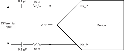 Figure 81. Analog Input Drive Circuit
8.2.2.2 Clock Input
The VSP5324-Q1 device can function with either single-ended or differential clock inputs. The device can automatically detect if a single-ended or differential clock is applied. To operate with a single-ended input clock, CLKP must be driven by a CMOS clock with CLKM tied to GND. Figure 82 and Figure 83 show the typical single-ended and differential clock termination schemes (respectively).
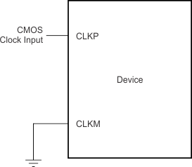 Figure 82. Single-Ended Clock Driving Circuit
 Figure 83. Differential Clock Driving Circuit
8.2.3 Application Curves
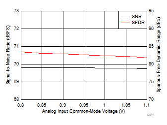
| ƒIN = 5 MHz | ||
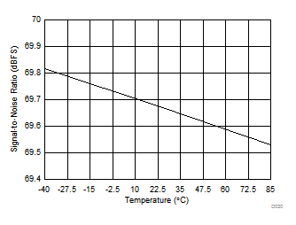
| A 0.7-VPP 5-MHz sine-wave input is applied on the INx_P pin | ||
| The INx_M pin is connected to the device VCM pin |