SLVSBN6A June 2013 – August 2015 DRV201A
PRODUCTION DATA.
- 1 Features
- 2 Applications
- 3 Description
- 4 Revision History
- 5 Pin Configuration and Functions
- 6 Specifications
-
7 Detailed Description
- 7.1 Overview
- 7.2 Functional Block Diagram
- 7.3 Feature Description
- 7.4 Device Functional Modes
- 7.5 Programming
- 7.6
Register Maps
- 7.6.1 Control Register (Address - 0x02h)
- 7.6.2 VCM MSB Current Control Register (VCM_Current_MSB) Address - 0x03h
- 7.6.3 VCM LSB Current Control Register (VCM_Current_lSB) Address - 0x04h
- 7.6.4 Status Register (Status) Address - 0x05h
- 7.6.5 Mode Register (Mode) Address - 0x06h
- 7.6.6 VCM Resonance Frequency Register (VCM_FREQ) Address - 0x07h
- 8 Application and Implementation
- 9 Power Supply Recommendations
- 10Layout
- 11Device and Documentation Support
- 12Mechanical, Packaging, and Orderable Information
Package Options
Mechanical Data (Package|Pins)
- YMB|6
Thermal pad, mechanical data (Package|Pins)
Orderable Information
1 Features
- Configurable for Linear or PWM Mode VCM Current Generation
- High Efficiency PWM Current Control for VCM
- Advanced Ringing Compensation
- Integrated 10-bit D/A Converter for VCM Current Control
- Protection
- Open and Short-Circuit Detection
- Undervoltage Lockout (UVLO)
- Thermal Shutdown
- Internal Current Limit for VCM Driver
- 4-kV ESD-HBM
- I2C Interface
- Improved PWM-to-Linear Mode Setting Time vs. DRV201
- Improved EMC Performance vs. DRV201
- Improved PWM-to-Linear Mode Settling Time vs. DRV201
- Improved EMC Performance vs. DRV201
- Operating Temperature Range: -40ºC to 85ºC
- 6-Ball WCSP Package With 0.4-mm Pitch
- Max Die Size: 0.806 mm × 1.49 mm
- Max Package Height: 0.3 mm
2 Applications
- Cell Phone Auto Focus
- Digital Still Camera Auto Focus
- Iris and Exposure Controls
- Security Cameras
- Web and PC Cameras
- Actuator Controls
3 Description
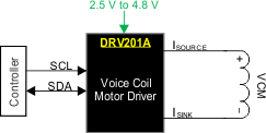
The DRV201A is an advanced voice coil motor driver for camera auto focus. It has an integrated D/A converter for setting the VCM current. VCM current is controlled with a fixed frequency PWM controller or a linear mode driver. Current generation can be selected via I2C register. The DRV201A has an integrated sense resistor for current regulation and the current can be controlled through I2C.
When changing the current in the VCM, the lens ringing is compensated with an advanced ringing compensation function. Ringing compensation reduces the needed time for auto focus significantly. The device also has VCM short and open protection functions.
Device Information(1)
| PART NUMBER | PACKAGE | BODY SIZE (NOM) |
|---|---|---|
| DRV201A | PicoStar (6) | 0.80 mm × 1.48 mm |
- For all available packages, see the orderable addendum at the end of the data sheet.
Simplified Schematic
