JAJSFR6A July   2018  – November 2018 ADS1219

PRODUCTION DATA.  

  1. 特長
  2. アプリケーション
  3. 概要
    1.     Device Images
      1.      電圧、電流、および温度監視アプリケーション
  4. 改訂履歴
  5. 概要(続き)
  6. Pin Configuration and Functions
    1.     Pin Functions
  7. Specifications
    1. 7.1 Absolute Maximum Ratings
    2. 7.2 ESD Ratings
    3. 7.3 Recommended Operating Conditions
    4. 7.4 Thermal Information
    5. 7.5 Electrical Characteristics
    6. 7.6 I2C Timing Requirements
    7. 7.7 I2C Switching Characteristics
    8. 7.8 Typical Characteristics
  8. Parameter Measurement Information
    1. 8.1 Noise Performance
  9. Detailed Description
    1. 9.1 Overview
    2. 9.2 Functional Block Diagram
    3. 9.3 Feature Description
      1. 9.3.1 Multiplexer
      2. 9.3.2 Rail-to-Rail Input Buffers and Programmable Gain Stage
      3. 9.3.3 Voltage Reference
      4. 9.3.4 Modulator and Internal Oscillator
      5. 9.3.5 Digital Filter
      6. 9.3.6 Conversion Times
      7. 9.3.7 Offset Calibration
    4. 9.4 Device Functional Modes
      1. 9.4.1 Power-Up and Reset
        1. 9.4.1.1 Power-On Reset
        2. 9.4.1.2 RESET Pin
        3. 9.4.1.3 Reset by Command
      2. 9.4.2 Conversion Modes
        1. 9.4.2.1 Single-Shot Conversion Mode
        2. 9.4.2.2 Continuous Conversion Mode
      3. 9.4.3 Power-Down Mode
    5. 9.5 Programming
      1. 9.5.1 I2C Interface
        1. 9.5.1.1 I2C Address
        2. 9.5.1.2 Serial Clock (SCL) and Serial Data (SDA)
        3. 9.5.1.3 Data Ready (DRDY)
        4. 9.5.1.4 Interface Speed
        5. 9.5.1.5 Data Transfer Protocol
        6. 9.5.1.6 I2C General Call (Software Reset)
        7. 9.5.1.7 Timeout
      2. 9.5.2 Data Format
      3. 9.5.3 Commands
        1. 9.5.3.1 Command Latching
        2. 9.5.3.2 RESET (0000 011x)
        3. 9.5.3.3 START/SYNC (0000 100x)
        4. 9.5.3.4 POWERDOWN (0000 001x)
        5. 9.5.3.5 RDATA (0001 xxxx)
        6. 9.5.3.6 RREG (0010 0rxx)
        7. 9.5.3.7 WREG (0100 00xx dddd dddd)
      4. 9.5.4 Reading Data and Monitoring for New Conversion Results
    6. 9.6 Register Map
      1. 9.6.1 Configuration and Status Registers
      2. 9.6.2 Register Descriptions
        1. 9.6.2.1 Configuration Register (address = 0h) [reset = 00h]
          1. Table 10. Configuration Register Field Descriptions
        2. 9.6.2.2 Status Register (address = 1h) [reset = 00h]
          1. Table 11. Status Register Field Descriptions
  10. 10Application and Implementation
    1. 10.1 Application Information
      1. 10.1.1 Interface Connections
      2. 10.1.2 Connecting Multiple Devices on the Same I2C Bus
      3. 10.1.3 Unused Inputs and Outputs
      4. 10.1.4 Analog Input Filtering
      5. 10.1.5 External Reference and Ratiometric Measurements
      6. 10.1.6 Establishing Proper Limits on the Absolute Input Voltage
      7. 10.1.7 Pseudo Code Example
    2. 10.2 Typical Application
      1. 10.2.1 Design Requirements
      2. 10.2.2 Detailed Design Procedure
        1. 10.2.2.1 Voltage Monitoring
        2. 10.2.2.2 High-Side Current Measurement
        3. 10.2.2.3 Thermistor Measurement
        4. 10.2.2.4 Register Settings
      3. 10.2.3 Application Curve
  11. 11Power Supply Recommendations
    1. 11.1 Power-Supply Sequencing
    2. 11.2 Power-Supply Decoupling
  12. 12Layout
    1. 12.1 Layout Guidelines
    2. 12.2 Layout Example
  13. 13デバイスおよびドキュメントのサポート
    1. 13.1 デバイス・サポート
      1. 13.1.1 デベロッパー・ネットワークの製品に関する免責事項
    2. 13.2 ドキュメントのサポート
      1. 13.2.1 関連資料
    3. 13.3 ドキュメントの更新通知を受け取る方法
    4. 13.4 コミュニティ・リソース
    5. 13.5 商標
    6. 13.6 静電気放電に関する注意事項
    7. 13.7 Glossary
  14. 14メカニカル、パッケージ、および注文情報

パッケージ・オプション

メカニカル・データ(パッケージ|ピン)
サーマルパッド・メカニカル・データ
発注情報

Digital Filter

The device uses a linear-phase finite impulse response (FIR) digital filter that performs both filtering and decimation of the digital data stream coming from the modulator. The digital filter is automatically adjusted for the different data rates and always settles within a single cycle. The frequency responses of the digital filter are shown in Figure 28 to Figure 32 for different output data rates. The filter notches and output data rate scale proportionally with the clock frequency. The internal oscillator can vary over temperature as specified in the Electrical Characteristics table. The data rate or conversion time, respectively, and consequently also the filter notches vary proportionally.
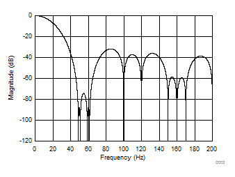
ADS1219 D002.gifFigure 28. Filter Response
(DR = 20 SPS)
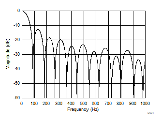
ADS1219 D004.gifFigure 30. Filter Response
(DR = 90 SPS)
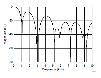
ADS1219 D008_sbas751.gifFigure 32. Filter Response
(DR = 1 kSPS)
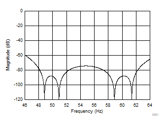
ADS1219 D001.gifFigure 29. Detailed View of the Filter Response
(DR = 20 SPS)
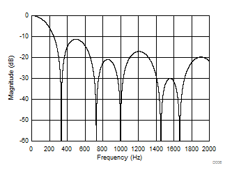
ADS1219 D006.gifFigure 31. Filter Response
(DR = 330 SPS)