JAJSFR6A July   2018  – November 2018 ADS1219

PRODUCTION DATA.  

  1. 特長
  2. アプリケーション
  3. 概要
    1.     Device Images
      1.      電圧、電流、および温度監視アプリケーション
  4. 改訂履歴
  5. 概要(続き)
  6. Pin Configuration and Functions
    1.     Pin Functions
  7. Specifications
    1. 7.1 Absolute Maximum Ratings
    2. 7.2 ESD Ratings
    3. 7.3 Recommended Operating Conditions
    4. 7.4 Thermal Information
    5. 7.5 Electrical Characteristics
    6. 7.6 I2C Timing Requirements
    7. 7.7 I2C Switching Characteristics
    8. 7.8 Typical Characteristics
  8. Parameter Measurement Information
    1. 8.1 Noise Performance
  9. Detailed Description
    1. 9.1 Overview
    2. 9.2 Functional Block Diagram
    3. 9.3 Feature Description
      1. 9.3.1 Multiplexer
      2. 9.3.2 Rail-to-Rail Input Buffers and Programmable Gain Stage
      3. 9.3.3 Voltage Reference
      4. 9.3.4 Modulator and Internal Oscillator
      5. 9.3.5 Digital Filter
      6. 9.3.6 Conversion Times
      7. 9.3.7 Offset Calibration
    4. 9.4 Device Functional Modes
      1. 9.4.1 Power-Up and Reset
        1. 9.4.1.1 Power-On Reset
        2. 9.4.1.2 RESET Pin
        3. 9.4.1.3 Reset by Command
      2. 9.4.2 Conversion Modes
        1. 9.4.2.1 Single-Shot Conversion Mode
        2. 9.4.2.2 Continuous Conversion Mode
      3. 9.4.3 Power-Down Mode
    5. 9.5 Programming
      1. 9.5.1 I2C Interface
        1. 9.5.1.1 I2C Address
        2. 9.5.1.2 Serial Clock (SCL) and Serial Data (SDA)
        3. 9.5.1.3 Data Ready (DRDY)
        4. 9.5.1.4 Interface Speed
        5. 9.5.1.5 Data Transfer Protocol
        6. 9.5.1.6 I2C General Call (Software Reset)
        7. 9.5.1.7 Timeout
      2. 9.5.2 Data Format
      3. 9.5.3 Commands
        1. 9.5.3.1 Command Latching
        2. 9.5.3.2 RESET (0000 011x)
        3. 9.5.3.3 START/SYNC (0000 100x)
        4. 9.5.3.4 POWERDOWN (0000 001x)
        5. 9.5.3.5 RDATA (0001 xxxx)
        6. 9.5.3.6 RREG (0010 0rxx)
        7. 9.5.3.7 WREG (0100 00xx dddd dddd)
      4. 9.5.4 Reading Data and Monitoring for New Conversion Results
    6. 9.6 Register Map
      1. 9.6.1 Configuration and Status Registers
      2. 9.6.2 Register Descriptions
        1. 9.6.2.1 Configuration Register (address = 0h) [reset = 00h]
          1. Table 10. Configuration Register Field Descriptions
        2. 9.6.2.2 Status Register (address = 1h) [reset = 00h]
          1. Table 11. Status Register Field Descriptions
  10. 10Application and Implementation
    1. 10.1 Application Information
      1. 10.1.1 Interface Connections
      2. 10.1.2 Connecting Multiple Devices on the Same I2C Bus
      3. 10.1.3 Unused Inputs and Outputs
      4. 10.1.4 Analog Input Filtering
      5. 10.1.5 External Reference and Ratiometric Measurements
      6. 10.1.6 Establishing Proper Limits on the Absolute Input Voltage
      7. 10.1.7 Pseudo Code Example
    2. 10.2 Typical Application
      1. 10.2.1 Design Requirements
      2. 10.2.2 Detailed Design Procedure
        1. 10.2.2.1 Voltage Monitoring
        2. 10.2.2.2 High-Side Current Measurement
        3. 10.2.2.3 Thermistor Measurement
        4. 10.2.2.4 Register Settings
      3. 10.2.3 Application Curve
  11. 11Power Supply Recommendations
    1. 11.1 Power-Supply Sequencing
    2. 11.2 Power-Supply Decoupling
  12. 12Layout
    1. 12.1 Layout Guidelines
    2. 12.2 Layout Example
  13. 13デバイスおよびドキュメントのサポート
    1. 13.1 デバイス・サポート
      1. 13.1.1 デベロッパー・ネットワークの製品に関する免責事項
    2. 13.2 ドキュメントのサポート
      1. 13.2.1 関連資料
    3. 13.3 ドキュメントの更新通知を受け取る方法
    4. 13.4 コミュニティ・リソース
    5. 13.5 商標
    6. 13.6 静電気放電に関する注意事項
    7. 13.7 Glossary
  14. 14メカニカル、パッケージ、および注文情報

パッケージ・オプション

メカニカル・データ(パッケージ|ピン)
サーマルパッド・メカニカル・データ
発注情報

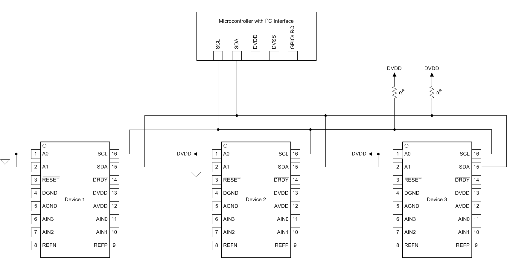
Connecting Multiple Devices on the Same I2C Bus

Up to 16 ADS1219 devices can be connected to a single I2C bus by using different address pin configurations for each device. Use the address pins, A0 and A1, to set the ADS1219 to one of 16 different I2C addresses. Figure 44 shows an example with three ADS1219 devices on the same I2C bus. One set of pullup resistors is required per bus line. If needed, decrease the pullup resistor values to compensate for the additional bus capacitance presented by multiple devices and increased line length.
ADS1219 ai_multi_device_connection_bas924.gifFigure 44. Connecting Multiple ADS1219 Devices on the Same I2C Bus