JAJSEC4E September   2012  – January 2018

PRODUCTION DATA.  

  1. 特長
  2. アプリケーション
  3. 概要
    1.     代表的なアプリケーション回路
  4. 改訂履歴
  5. 概要(続き)
  6. Device Comparisons
  7. Pin Configuration and Functions
    1.     Pin Functions
  8. Specifications
    1. 8.1 Absolute Maximum Ratings
    2. 8.2 ESD Ratings
    3. 8.3 Recommended Operating Conditions
    4. 8.4 Thermal Information
    5. 8.5 Electrical Characteristics
    6. 8.6 Timing Requirements
    7. 8.7 Typical Characteristics
  9. Detailed Description
    1. 9.1 Overview
    2. 9.2 Functional Block Diagrams
    3. 9.3 Operational Flow Chart
    4. 9.4 Feature Description
      1. 9.4.1 Input Voltage Protection
        1. 9.4.1.1 Input Overvoltage Protection
        2. 9.4.1.2 Bad Adaptor Detection/Rejection
        3. 9.4.1.3 Sleep Mode
        4. 9.4.1.4 Input Voltage Based DPM (Special Charger Voltage Threshold)
      2. 9.4.2 Battery Protection
        1. 9.4.2.1 Output Overvoltage Protection
        2. 9.4.2.2 Battery Detection at Power Up in DEFAULT Mode
        3. 9.4.2.3 Battery Short Protection
        4. 9.4.2.4 Battery Detection in Host Mode
      3. 9.4.3 DEFAULT Mode
      4. 9.4.4 USB Friendly Power Up
      5. 9.4.5 Input Current Limiting At Power Up
    5. 9.5 Device Functional Modes
      1. 9.5.1 Charge Mode Operation
        1. 9.5.1.1 Charge Profile
      2. 9.5.2 PWM Controller in Charge Mode
      3. 9.5.3 Battery Charging Process
      4. 9.5.4 Thermal Regulation and Protection
      5. 9.5.5 Charge Status Output, STAT Pin
      6. 9.5.6 Control Bits in Charge Mode
        1. 9.5.6.1 CE Bit (Charge Mode)
        2. 9.5.6.2 RESET Bit
        3. 9.5.6.3 OPA_Mode Bit
      7. 9.5.7 Control Pins in Charge Mode
        1. 9.5.7.1 CD Pin (Charge Disable)
      8. 9.5.8 BOOST Mode Operation
        1. 9.5.8.1 PWM Controller in Boost Mode
        2. 9.5.8.2 Boost Start Up
        3. 9.5.8.3 PFM Mode at Light Load
        4. 9.5.8.4 Protection in Boost Mode
          1. 9.5.8.4.1 Output Overvoltage Protection
          2. 9.5.8.4.2 Output Overload Protection
          3. 9.5.8.4.3 Battery Overvoltage Protection
        5. 9.5.8.5 STAT Pin in Boost Mode
      9. 9.5.9 High Impedance (Hi-Z) Mode
    6. 9.6 Programming
      1. 9.6.1 Serial Interface Description
        1. 9.6.1.1 F/S Mode Protocol
        2. 9.6.1.2 H/S Mode Protocol
        3. 9.6.1.3 I2C Update Sequence
        4. 9.6.1.4 Slave Address Byte
        5. 9.6.1.5 Register Address Byte
    7. 9.7 Register Description
  10. 10Application and Implementation
    1. 10.1 Application Information
      1. 10.1.1 Typical Application
        1. 10.1.1.1 Design Requirements
        2. 10.1.1.2 Detailed Design Procedure
      2. 10.1.2 Charge Current Sensing Resistor Selection Guidelines
      3. 10.1.3 Output Inductor and Capacitance Selection Guidelines
    2. 10.2 Typical Performance Curves
  11. 11Power Supply Recommendations
    1. 11.1 System Load After Sensing Resistor
      1. 11.1.1 The Advantages:
      2. 11.1.2 Design Requirements and Potential Issues:
  12. 12Layout
    1. 12.1 Layout Guidelines
    2. 12.2 Layout Example
  13. 13デバイスおよびドキュメントのサポート
    1. 13.1 ドキュメントのサポート
      1. 13.1.1 デベロッパー・ネットワークの製品に関する免責事項
    2. 13.2 ドキュメントの更新通知を受け取る方法
    3. 13.3 コミュニティ・リソース
    4. 13.4 商標
    5. 13.5 静電気放電に関する注意事項
    6. 13.6 Glossary
  14. 14メカニカル、パッケージ、および注文情報
    1. 14.1 パッケージ概要
      1. 14.1.1 チップ・スケール・パッケージの寸法

パッケージ・オプション

メカニカル・データ(パッケージ|ピン)
サーマルパッド・メカニカル・データ
発注情報

Bad Adaptor Detection/Rejection

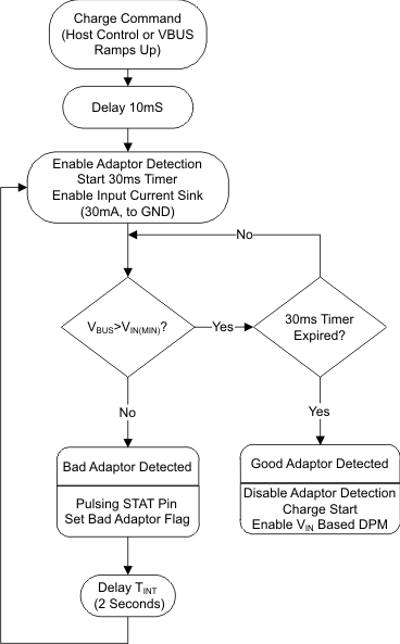
Although not shown in Figure 14, at power-on-reset (POR) of VBUS, the IC performs the bad adaptor detection by applying a current sink to VBUS. If the VBUS is higher than VIN(MIN) for 30ms, the adaptor is good and the charge process begins. Otherwise, if the VBUS drops below VIN(MIN), a bad adaptor is detected. Then, the IC disables the current sink, sends a send fault pulse in FAULT pin and sets the bad adaptor flag (B2 - B0 = 011 for Register 00H). After a delay of TINT, the IC repeats the adaptor detection process, as shown in Figure 15 and Figure 16.
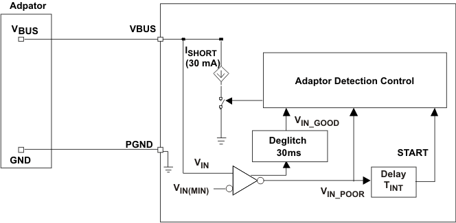
bq24157 adap_det_lusa27.gifFigure 15. Bad Adaptor Detection Circuit
bq24157 adap_flo_lusa27.gifFigure 16. Bad Adaptor Detection Scheme Flow Chart