JAJSGQ2F August   2013  – March 2019

PRODUCTION DATA.  

  1. 特長
  2. アプリケーション
  3. 概要
    1.     Device Images
      1.      概略回路図
      2.      充電器の効率
  4. 改訂履歴
  5. Pin Configuration and Functions
    1.     Pin Functions
  6. Specifications
    1. 6.1 Absolute Maximum Ratings
    2. 6.2 ESD Ratings
    3. 6.3 Recommended Operating Conditions
    4. 6.4 Thermal Information
    5. 6.5 Electrical Characteristics
    6. 6.6 Typical Characteristics
  7. Detailed Description
    1. 7.1 Overview
    2. 7.2 Functional Block Diagram
    3. 7.3 Feature Description
      1. 7.3.1 Maximum Power Point Tracking
      2. 7.3.2 Battery Undervoltage Protection
      3. 7.3.3 Battery Overvoltage Protection
      4. 7.3.4 Battery Voltage in Operating Range (VBAT_OK Output)
      5. 7.3.5 Push-Pull Multiplexer Drivers
      6. 7.3.6 Nano-Power Management and Efficiency
    4. 7.4 Device Functional Modes
      1. 7.4.1 Main Boost Charger Disabled (Ship Mode) - (VSTOR > VSTOR_CHGEN and EN = HIGH)
      2. 7.4.2 Cold-Start Operation (VSTOR < VSTOR_CHGEN, VIN_DC > VIN(CS) and PIN > PIN(CS))
      3. 7.4.3 Main Boost Charger Enabled (VSTOR > VSTOR_CHGEN, VIN_DC > VIN(DC) and EN = LOW )
      4. 7.4.4 Thermal Shutdown
  8. Application and Implementation
    1. 8.1 Application Information
      1. 8.1.1 Energy Harvester Selection
      2. 8.1.2 Storage Element Selection
      3. 8.1.3 Inductor Selection
      4. 8.1.4 Capacitor Selection
        1. 8.1.4.1 VREF_SAMP Capacitance
        2. 8.1.4.2 VIN_DC Capacitance
        3. 8.1.4.3 VSTOR Capacitance
        4. 8.1.4.4 Additional Capacitance on VSTOR or VBAT_SEC
    2. 8.2 Typical Applications
      1. 8.2.1 Solar Application Circuit
        1. 8.2.1.1 Design Requirements
        2. 8.2.1.2 Detailed Design Procedure
        3. 8.2.1.3 Application Performance Plots
      2. 8.2.2 TEG Application Circuit
      3. 8.2.3 Design Requirements
        1. 8.2.3.1 Detailed Design Procedure
        2. 8.2.3.2 Application Performance Plots
      4. 8.2.4 Piezoelectric Application Circuit
        1. 8.2.4.1 Design Requirements
        2. 8.2.4.2 Detailed Design Procedure
        3. 8.2.4.3 Application Curves
  9. Power Supply Recommendations
  10. 10Layout
    1. 10.1 Layout Guidelines
    2. 10.2 Layout Example
    3. 10.3 Thermal Considerations
  11. 11デバイスおよびドキュメントのサポート
    1. 11.1 デバイス・サポート
      1. 11.1.1 デベロッパー・ネットワークの製品に関する免責事項
      2. 11.1.2 Zipファイル
    2. 11.2 ドキュメントのサポート
      1. 11.2.1 関連資料
    3. 11.3 ドキュメントの更新通知を受け取る方法
    4. 11.4 コミュニティ・リソース
    5. 11.5 商標
    6. 11.6 静電気放電に関する注意事項
    7. 11.7 Glossary
  12. 12メカニカル、パッケージ、および注文情報

パッケージ・オプション

メカニカル・データ(パッケージ|ピン)
サーマルパッド・メカニカル・データ
発注情報

Application Performance Plots

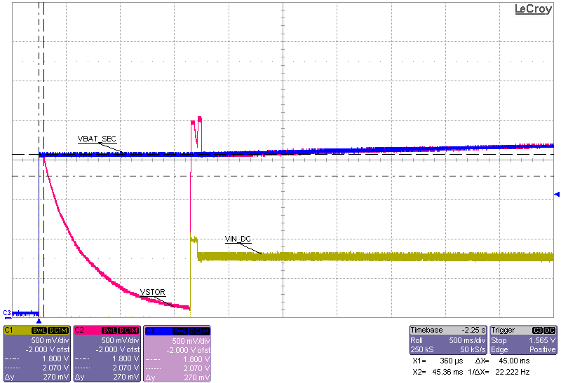
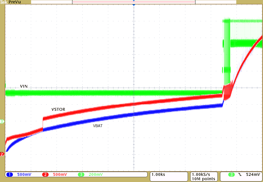
bq25505 app1_startup_1VIN_8p5ma_100kohm_slusbj3.png
Sourcemeter with VSOURCE = 1.0 V and compliance of 8.5 mA subsequently applied to VIN_DC
VBAT_SEC = 0.1 F capacitor charged to 2.0 V
Resistance on VSTOR = 100 kΩ
Figure 17. Startup by Battery Attach With Almost Depleted Storage Element
bq25505 app1_mppt_ov_4p2v_3vstor_2p0vin_42p6ma_slusbj3.png
VIN_DC = sourcemeter with VSOURCE = 2.0 V and compliance of 43 mA
VBAT_SEC = sourcemeter with VSOURCE = 3.0 V and compliance of 1 A
Figure 19. MPPT Operation
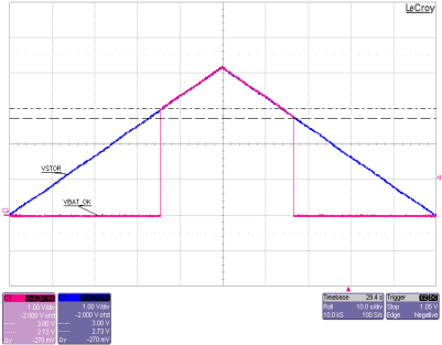
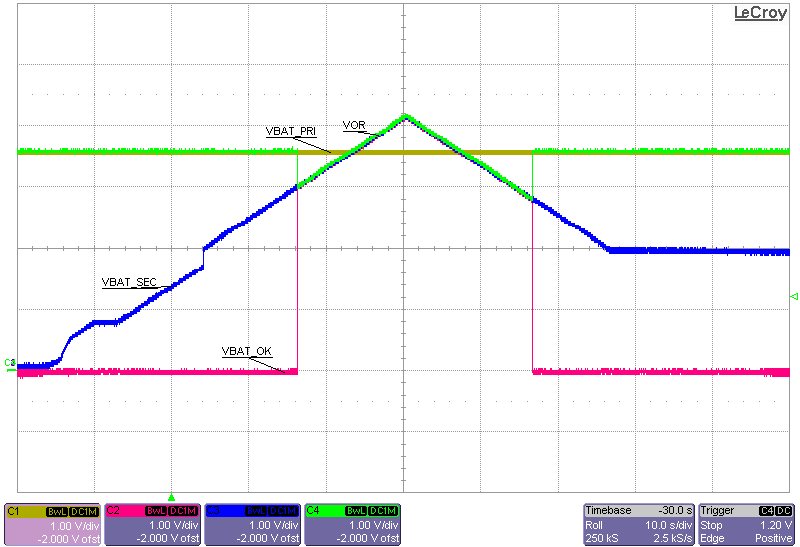
bq25505 bq25570_bq25505-vbat-ok1_lusbh2.gif
VIN_DC = 1.5 V with 75 Ω series resistance
No storage element on VBAT_SEC or VBAT_PRI
VSTOR artifically ramped from 0 V to 4.2 V to 0 V using a power amp driven by a function generator
Figure 21. VBAT_OK Operation
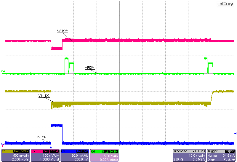
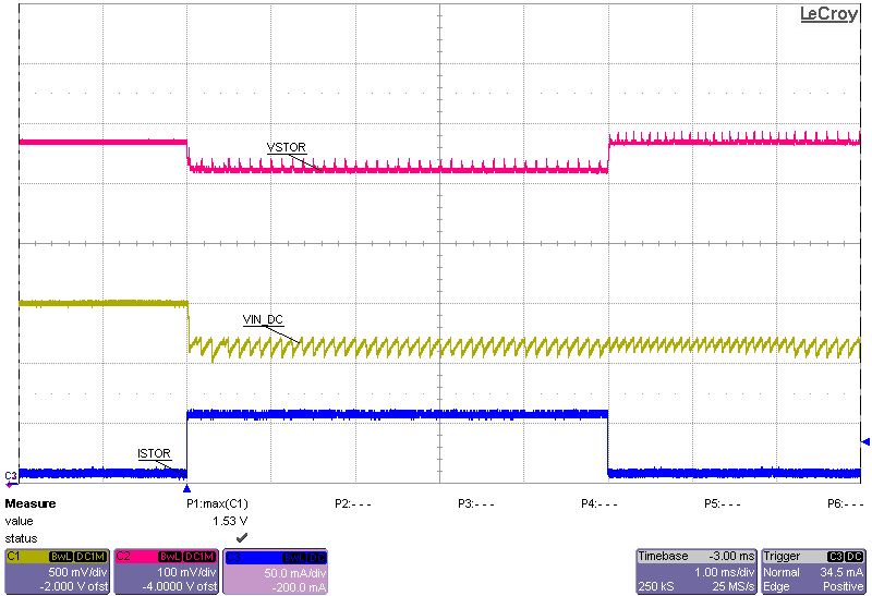
bq25505 bq25505-ds21_50MA-LD_TRN.png
VIN_DC = 1.5 V with 75 Ω series resistance
VBAT = 4.2 V charged 0.5 F capacitor
R(VSTOR) = open to 84 Ω to open
Figure 23. 50 mA Load Transient on VSTOR - Zoom Out
bq25505 bq25505-ds27-multi-pri-hi-3P6V.png
VIN_DC = 1.5 V with 75 Ω series resistance; VBAT _PRI = 3.6 V power supply
0.5 F super capacitor on VBAT_SEC; 1kΩ load on output of MUX FETs (VOR)
VSTOR artifically ramped from 0 V to 4.2 V using a function generator
Figure 25. MUX Signals When VBAT_SEC > VBAT_OK Threshold
bq25505 IIN_1mA_VOC_1p2V_CSTOR_100uF_VBAT_supcap_0p12F_1.png
VIN_DC = source meter with 1.2 V compliance and ISC = 1 mA
120 mF super capacitor on VBAT_SEC
Figure 27. Charging a Super Capacitor on VBAT
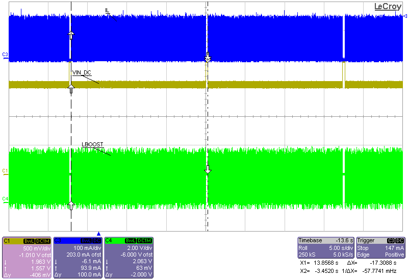
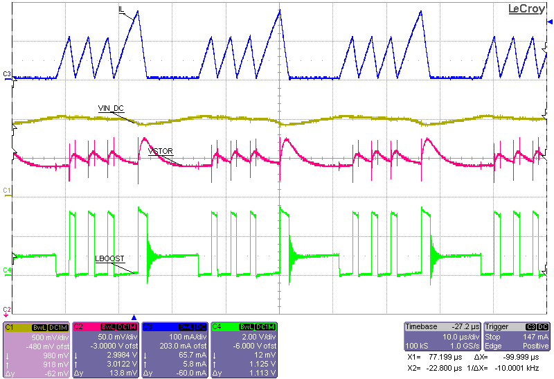
bq25505 app2_operation_ov_5p0v_3vstor_2p0vin_42p6ma_slusbj3.png
VIN_DC = sourcemeter with VSOURCE = 2.0 V and compliance of 43 mA
VBAT_SEC = sourcemeter with VSOURCE = 3.0 V and compliance of 1 A
IL = inductor current
Figure 18. Boost Charger Operational Waveforms
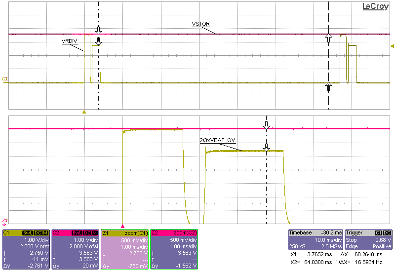
bq25505 app1_VRDIV_ov_4p2v_slusbj3.png
VIN_DC = sourcemeter with VSOURCE = 2.0 V and compliance of 43 mA
VBAT_SEC = sourcemeter with VSOURCE = 3.6 V and compliance of 1 A
Figure 20. VRDIV Waveform
bq25505 bq25505-ds20-50MA-LD_TRN.png
VIN_DC = 1.5 V with 75 Ω series resistance
VBAT = 4.2 V charged 0.5 F capacitor
R(VSTOR) = open to 84 Ω to open
Figure 22. 50 mA Load Transient on VSTOR
bq25505 bq25505-ds26-multi-out.png
VIN_DC = 1.5 V with 75 Ω series resistance; VBAT _PRI = 3.6 V power supply
0.5 F super capacitor on VBAT_SEC; 1kΩ load on output of MUX FETs (VOR)
VSTOR artifically ramped from 0 V to 4.2 V to 0 V using a function generator
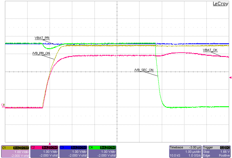
Figure 24. Multiplexer Output (VOR) as VBAT_SEC Crosses VBAT_OK Threshold
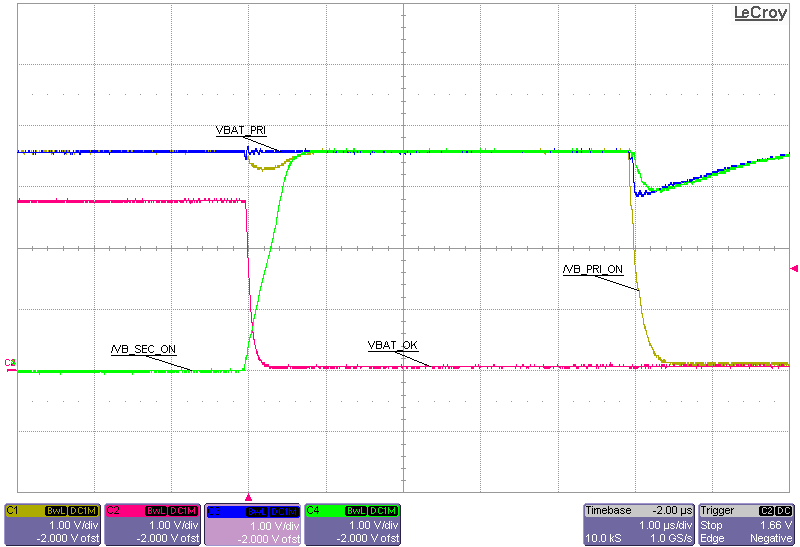
bq25505 bq25505-ds28-multi-pri-lo-3P6V.png
VIN_DC = 1.5 V with 75 Ω series resistance; VBAT _PRI = 3.6 V power supply
0.5 F super capacitor on VBAT_SEC; 1kΩ load on output of MUX FETs (VOR)
VSTOR artifically ramped from 4.2 V to 0 V using a function generator
Figure 26. MUX Signals When VBAT_SEC < VBAT_OK Threshold