JAJSHN4D June   2019  – December 2021 BQ25618 , BQ25619

PRODUCTION DATA  

  1. Features
  2. アプリケーション
  3. Description
  4. Revision History
  5. Description (continued)
  6. Pin Configuration and Functions
  7. Specifications
    1. 7.1 Absolute Maximum Ratings
    2. 7.2 ESD Ratings
    3. 7.3 Recommended Operating Conditions
    4. 7.4 Thermal Information
    5. 7.5 Thermal Information
    6. 7.6 Electrical Characteristics
    7. 7.7 Timing Requirements
    8. 7.8 Typical Characteristics
  8. Detailed Description
    1. 8.1 Overview
    2. 8.2 Functional Block Diagram
    3. 8.3 Feature Description
      1. 8.3.1  Power-On-Reset (POR)
      2. 8.3.2  Device Power Up From Battery Without Input Source
      3. 8.3.3  Power Up From Input Source
        1. 8.3.3.1 Power Up REGN LDO
        2. 8.3.3.2 Poor Source Qualification
        3. 8.3.3.3 Input Source Type Detection (IINDPM Threshold)
          1. 8.3.3.3.1 PSEL Pins Sets Input Current Limit
        4. 8.3.3.4 Input Voltage Limit Threshold Setting (VINDPM Threshold)
        5. 8.3.3.5 Power Up Converter in Buck Mode
        6. 8.3.3.6 HIZ Mode with Adapter Present
      4. 8.3.4  Boost Mode Operation From Battery
      5. 8.3.5  Power Path Management
        1. 8.3.5.1 Narrow VDC Architecture
        2. 8.3.5.2 Dynamic Power Management
        3. 8.3.5.3 Supplement Mode
      6. 8.3.6  Battery Charging Management
        1. 8.3.6.1 Autonomous Charging Cycle
        2. 8.3.6.2 Battery Charging Profile
        3. 8.3.6.3 Charging Termination
        4. 8.3.6.4 Thermistor Qualification
          1. 8.3.6.4.1 JEITA Guideline Compliance During Charging Mode
          2. 8.3.6.4.2 Boost Mode Thermistor Monitor During Battery Discharge Mode
        5. 8.3.6.5 Charging Safety Timer
      7. 8.3.7  Ship Mode and QON Pin
        1. 8.3.7.1 BATFET Disable (Enter Ship Mode)
        2. 8.3.7.2 BATFET Enable (Exit Ship Mode)
        3. 8.3.7.3 BATFET Full System Reset
      8. 8.3.8  Status Outputs (STAT, INT , PMID_GOOD)
        1. 8.3.8.1 Power Good Indicator (PG_STAT Bit)
        2. 8.3.8.2 Charging Status Indicator (STAT)
        3. 8.3.8.3 Interrupt to Host (INT)
        4. 8.3.8.4 PMID Voltage Indicator (PMID_GOOD)
      9. 8.3.9  Protections
        1. 8.3.9.1 Voltage and Current Monitoring in Buck Mode
          1. 8.3.9.1.1 Input Overvoltage Protection (ACOV)
          2. 8.3.9.1.2 System Overvoltage Protection (SYSOVP)
        2. 8.3.9.2 Voltage and Current Monitoring in Boost Mode
          1. 8.3.9.2.1 Boost Mode Overvoltage Protection
          2. 8.3.9.2.2 PMID Overcurrent Protection
        3. 8.3.9.3 Thermal Regulation and Thermal Shutdown
          1. 8.3.9.3.1 Thermal Protection in Buck Mode
          2. 8.3.9.3.2 Thermal Protection in Boost Mode
        4. 8.3.9.4 Battery Protection
          1. 8.3.9.4.1 Battery Overvoltage Protection (BATOVP)
          2. 8.3.9.4.2 Battery Overdischarge Protection
          3. 8.3.9.4.3 System Overcurrent Protection
      10. 8.3.10 Serial Interface
        1. 8.3.10.1 Data Validity
        2. 8.3.10.2 START and STOP Conditions
        3. 8.3.10.3 Byte Format
        4. 8.3.10.4 Acknowledge (ACK) and Not Acknowledge (NACK)
        5. 8.3.10.5 Slave Address and Data Direction Bit
        6. 8.3.10.6 Single Read and Write
        7. 8.3.10.7 Multi-Read and Multi-Write
    4. 8.4 Device Functional Modes
      1. 8.4.1 Host Mode and Default Mode
    5. 8.5 Register Maps
  9. Application and Implementation
    1. 9.1 Application Information
    2. 9.2 Typical Application
      1. 9.2.1 Design Requirements
      2. 9.2.2 Detailed Design Procedure
        1. 9.2.2.1 Inductor Selection
        2. 9.2.2.2 Input Capacitor and Resistor
        3. 9.2.2.3 Output Capacitor
      3. 9.2.3 Application Curves
  10. 10Power Supply Recommendations
  11. 11Layout
    1. 11.1 Layout Guidelines
    2. 11.2 Layout Example
  12. 12Device and Documentation Support
    1. 12.1 Device Support
      1. 12.1.1 Third-Party Products Disclaimer
    2. 12.2 Documentation Support
      1. 12.2.1 Related Documentation
    3. 12.3 Receiving Notification of Documentation Updates
    4. 12.4 サポート・リソース
    5. 12.5 Trademarks
    6. 12.6 Electrostatic Discharge Caution
    7. 12.7 Glossary
  13. 13Mechanical, Packaging, and Orderable Information

パッケージ・オプション

メカニカル・データ(パッケージ|ピン)
サーマルパッド・メカニカル・データ
発注情報
JEITA Guideline Compliance During Charging Mode

To improve the safety of charging Li-ion batteries, the JEITA guideline was released on April 20, 2007. The guideline emphasized the importance of avoiding a high charge current and high charge voltage at certain low and high temperature ranges.

To initiate a charge cycle, the voltage on TS pin, as a percentage of VREGN, must be within the VT1_FALL% to VT5_RISE% thresholds. If the TS voltage percentage exceeds the T1-T5 range, the controller suspends charging, a TS fault is reported and waits until the battery temperature is within the T1-T5 range.

At cool temperature (T1-T2), the charge current is reduced to a programmable fast charge current (0%, 20% default, 50%, 100% of ICHG, by JEITA_ISET). At warm temperature (T3-T5), the charge voltage is reduced to 4.1 V or kept at VREG (JEITA_VSET), and the charge current can be reduced to a programmable level (0%, 20%, 50%, 100% default). Battery termination is disabled in T3-T5. The charger provides more flexible settings on a T2 and T3 threshold as well to program the temperature profile beyond JEITA. When T1 is set to 0°C and T5 is set to 60°C, T2 can be programmed to 5.5°C/10°C (default)/15°C/20°C, and T3 can be programmed to 40°C/45.5°C (default)/50.5°C/54.5°C.

When the charger does not need to monitor the NTC, the host sets the TS_IGNORE bit to 1 to ignore the TS pin condition during charging and Boost mode. If the TS_IGNORE bit is set to 1, the TS pin is ignored and the charger ignores the TS pin input. In this case, the NTC_FAULT bits are 000 to report normal TS status.

GUID-7CC9E969-BCCD-4632-81A2-5810C4A1DF77-low.gif Figure 8-4 JEITA Profile


Equation 1 through Equation 2 describe how to calculate resistor divider values on the TS pin.

GUID-57F57A94-068C-4DDC-A081-3234563D4747-low.gifFigure 8-5 TS Pin Resistor Network
Equation 1. GUID-4C1FF4ED-DF10-4FF9-8795-AB0970A5B6FF-low.gif
Equation 2. GUID-7D9C191F-6571-4BBD-81C6-5D2E2AB0DC6C-low.gif

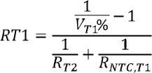
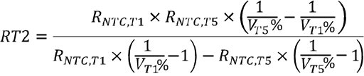
In the equations above, RNTC, T1 is the NTC thermistor resistance value at temperature T1 and RNTC, T5 is the NTC thermistor resistance value at temperature T5. Selecting a 0°C to 60°C range for a Li-ion or Li-polymer battery then:

  • RNTC,T1 = 27.28 kΩ (0°C)
  • RNTC,T5 = 3.02 kΩ (60°C)
  • RT1 = 5.3 kΩ
  • RT2 = 31.14 kΩ