JAJSF16D march   2013  – september 2020 BQ51013B

PRODUCTION DATA  

  1.   1
  2. 特長
  3. アプリケーション
  4. 概要
  5. Revision History
  6. Device Comparison Table
  7. Pin Configuration and Functions
    1.     Pin Functions
  8. Specifications
    1. 7.1 Absolute Maximum Ratings
    2. 7.2 ESD Ratings
    3. 7.3 Recommended Operating Conditions
    4. 7.4 Thermal Information
    5. 7.5 Electrical Characteristics
    6. 7.6 Typical Characteristics
  9. Detailed Description
    1. 8.1 Overview
    2. 8.2 Functional Block Diagram
    3. 8.3 Feature Description
      1. 8.3.1  Details of a Qi Wireless Power System and BQ51013 Power Transfer Flow Diagrams
      2. 8.3.2  Dynamic Rectifier Control
      3. 8.3.3  Dynamic Efficiency Scaling
      4. 8.3.4  RILIM Calculations
      5. 8.3.5  Input Overvoltage
      6. 8.3.6  Adapter Enable Functionality and EN1/EN2 Control
      7. 8.3.7  End Power Transfer Packet (WPC Header 0x02)
      8. 8.3.8  Status Outputs
      9. 8.3.9  WPC Communication Scheme
      10. 8.3.10 Communication Modulator
      11. 8.3.11 Adaptive Communication Limit
      12. 8.3.12 Synchronous Rectification
      13. 8.3.13 Temperature Sense Resistor Network (TS)
      14. 8.3.14 3-State Driver Recommendations for the TS/CTRL Pin
      15. 8.3.15 Thermal Protection
      16. 8.3.16 WPC v1.2 Compliance – Foreign Object Detection
      17. 8.3.17 Receiver Coil Load-Line Analysis
    4. 8.4 Device Functional Modes
  10. Application and Implementation
    1. 9.1 Application Information
    2. 9.2 Typical Applications
      1. 9.2.1 BQ51013B Wireless Power Receiver Used as a Power Supply
        1. 9.2.1.1 Design Requirements
        2. 9.2.1.2 Detailed Design Procedure
          1. 9.2.1.2.1 Using The BQ51013b as a Wireless Power Supply: (See )
          2. 9.2.1.2.2 Series and Parallel Resonant Capacitor Selection
          3. 9.2.1.2.3 Recommended RX Coils
          4. 9.2.1.2.4 COMM, CLAMP, and BOOT Capacitors
          5. 9.2.1.2.5 Control Pins and CHG
          6. 9.2.1.2.6 Current Limit and FOD
          7. 9.2.1.2.7 RECT and OUT Capacitance
        3. 9.2.1.3 Application Curves
      2. 9.2.2 Dual Power Path: Wireless Power and DC Input
        1. 9.2.2.1 Design Requirements
        2. 9.2.2.2 Detailed Design Procedure
        3. 9.2.2.3 Application Curves
      3. 9.2.3 Wireless and Direct Charging of a Li-Ion Battery at 800 mA
        1. 9.2.3.1 Design Requirements
        2. 9.2.3.2 Detailed Design Procedure
        3. 9.2.3.3 Application Curves
  11. 10Power Supply Recommendations
  12. 11Layout
    1. 11.1 Layout Guidelines
    2. 11.2 Layout Example
  13. 12Device and Documentation Support
    1. 12.1 Device Support
      1. 12.1.1 サード・パーティ製品に関する免責事項
      2. 12.1.2 Development Support
    2. 12.2 ドキュメントの更新通知を受け取る方法
    3. 12.3 サポート・リソース
    4. 12.4 Trademarks
    5. 12.5 静電気放電に関する注意事項
    6. 12.6 用語集
  14. 13Mechanical, Packaging, and Orderable Information

パッケージ・オプション

メカニカル・データ(パッケージ|ピン)
サーマルパッド・メカニカル・データ
発注情報

Typical Characteristics

GUID-0D625EF6-A6DF-4CB0-83CE-9977317560F5-low.gif
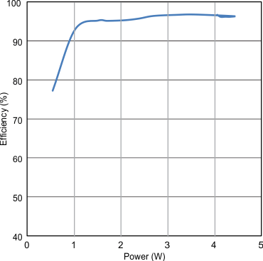
Input: RX AC powerOutput: RX RECT power
Efficiency: Output Power / Input Power
Figure 7-1 Rectifier Efficiency
GUID-F0F8B73C-919C-4ADD-B4F2-C0394AD48FED-low.gif
Input: TX DC power Output: RX RECT power
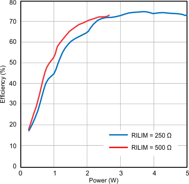
Plot: Output Power / Input Power
Figure 7-3 Light Load System Efficiency Improvement Due to Dynamic Efficiency Scaling Feature (1)
GUID-0B974303-8441-4DC5-B03D-4203649B3B87-low.gif
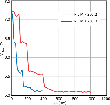
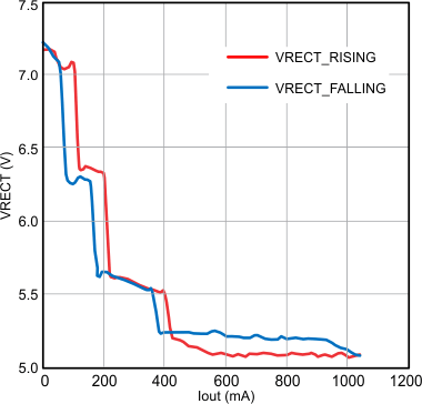
RILIM = 250 Ω and 750 Ω
Figure 7-5 Impact of Maximum Current setting (RILIM) on Rectifier Voltage (VRECT)
GUID-74CFB8C1-1FD1-44DF-A1CD-1CDE5430BDFC-low.gif
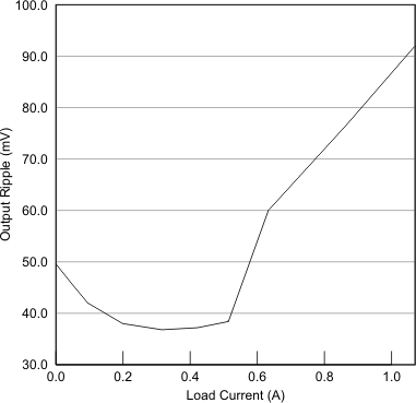
COUT = 1 µf Without Communication
Figure 7-7 Impact of Load Current on Output Ripple
GUID-D6D70DDB-1A55-497F-A4AF-7F5D562B0340-low.gif
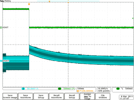
Figure 7-9 1-A Instantaneous Load Dump (2)
GUID-9554A270-C510-4038-9032-EAE7FAB5BBE2-low.png
Figure 7-11 1-A Load Dump Full System Response
GUID-676CCA3D-62E9-4038-9F6D-D45555F38286-low.gif
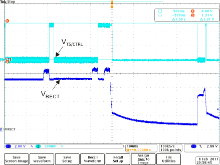
Figure 7-13 TS Fault
GUID-CD5B7EDD-D045-40BE-A611-79CCA2EB3A82-low.gif
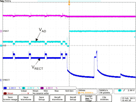
Figure 7-15 Adapter Insertion (VAD = 10 V) Illustrating Break-Before-Make Operation
GUID-CC24B826-D4CA-4E39-8A0B-53B461E06EB3-low.gif
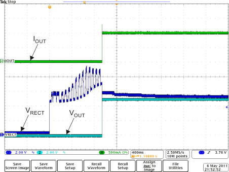
Figure 7-17 BQ51013B Typical Start-Up With a 1-A System Load
GUID-23B61087-1F6B-4705-A393-E9E916198662-low.gif
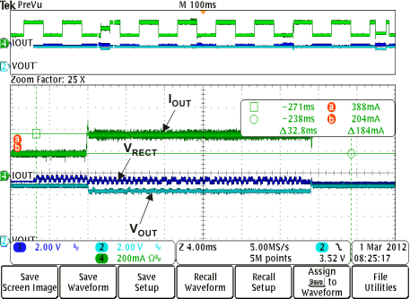
Figure 7-19 Adaptive Communication Limit Event Where the Current Limit is IOUT + 50 mA (IOUT-DC > 300 mA)
GUID-75DE2A99-2080-4AC6-8DF7-452915461232-low.gif
Input: TX DC powerOutput: RX RECT power
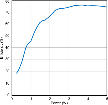
Efficiency: Output Power / Input Power
Figure 7-2 System Efficiency From DC Input to DC Output
GUID-108B7DDF-F7A2-48B0-B0AF-ED1B8984753B-low.gif
RILIM = 250 Ω
Figure 7-4 Impact of Load Current ( ILOAD) on Rectifier Voltage (VRECT)
GUID-0898C7AE-F68A-4837-BAA6-9077D3C10798-low.gif
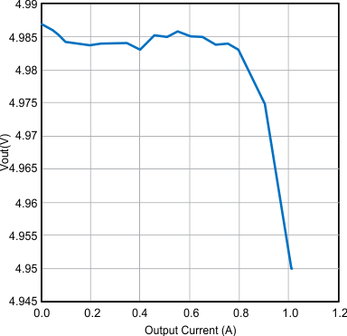
Maximum Current = 1 A
Figure 7-6 Impact of Load Current on Output Voltage
GUID-33EF9FF1-F65A-47D5-8D58-70658EF31882-low.gif
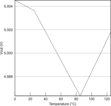
Figure 7-8 VOUT vs Temperature
GUID-067E0AE7-3CBD-4129-81D5-166AADA3263F-low.png
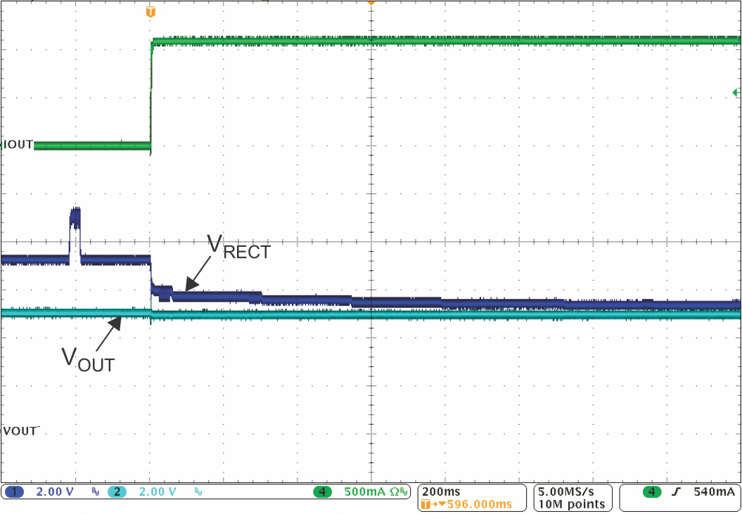
Figure 7-10 1-A Load Step Full System Response
GUID-A86427D7-929C-4714-87F2-681161E2D3D7-low.gif
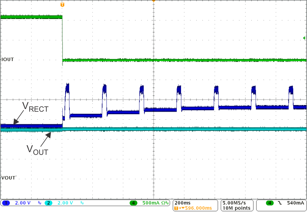
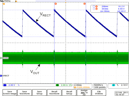
Figure 7-12 Rectifier Overvoltage Clamp (fop = 110 kHz)
GUID-734A0A40-F030-4429-A6A5-7E008C6BD376-low.gif
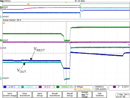
Figure 7-14 Adapter Insertion (VAD = 10 V)
GUID-42327BA5-D7F5-4807-9A15-E0114D5D623E-low.gif
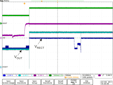
Figure 7-16 On-the-Go Enabled (VOTG = 3.5 V) (3)
GUID-EC9C39F0-1B9B-47E5-9F92-89C0A3D82DC9-low.gif
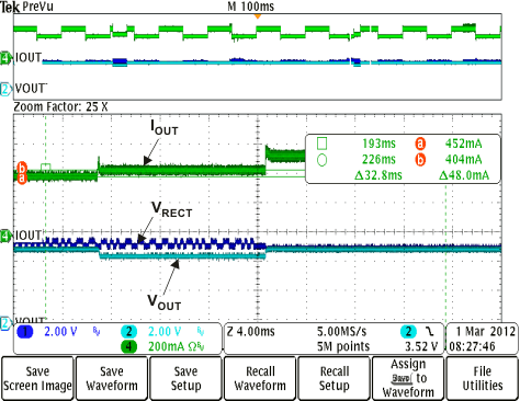
Figure 7-18 Adaptive Communication Limit Event Where the 400 mA Current Limit is Enabled (IOUT-DC < 300 mA)
GUID-0F42805D-7B1F-4E28-80AA-C27D052E68BB-low.gif
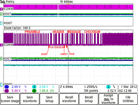
Figure 7-20 RX Communication Packet Structure
  1. Efficiency measured from DC input to the transmitter to DC output of the receiver. The BQ500210EVM-689 TX was used for these measurements. Measurement subject to change if an alternate TX is used.
  2. Total droop experienced at the output is dependent on receiver coil design. The output impedance must be low enough at that particular operating frequency in order to not collapse the rectifier below 5 V.
  3. On-the-go mode is enabled by driving EN1 high. In this test, the external PMOS is connected between the output of the BQ51013B device and the AD pin; therefore, any voltage source on the output is supplied to the AD pin.