SLUSB42F July 2012 – June 2017
PRODUCTION DATA.
- 1 Features
- 2 Applications
- 3 Description
- 4 Revision History
- 5 Device Options
- 6 Pin Configuration and Functions
- 7 Specifications
-
8 Detailed Description
- 8.1 Overview
- 8.2 Functional Block Diagram
- 8.3
Feature Description
- 8.3.1 Using the bq5105x as a Wireless Li-Ion/Li-Pol Battery Charger (With Reference to )
- 8.3.2 Details of a Qi Wireless Power System and bq5105xB Power Transfer Flow Diagrams
- 8.3.3 Battery Charge Profile
- 8.3.4
Battery Charging Process
- 8.3.4.1 Precharge Mode (VBAT ≤ VLOWV)
- 8.3.4.2 Fast Charge Mode / Constant Voltage Mode
- 8.3.4.3 Battery Charge Current Setting Calculations
- 8.3.4.4 Battery-Charger Safety and JEITA Guidelines
- 8.3.4.5 Input Overvoltage
- 8.3.4.6 End Power Transfer Packet (WPC Header 0x02)
- 8.3.4.7 Status Output
- 8.3.4.8 Communication Modulator
- 8.3.4.9 Adaptive Communication Limit
- 8.3.4.10 Synchronous Rectification
- 8.3.4.11 Internal Temperature Sense (TS Function of the TS/CTRL Pin)
- 8.3.4.12 WPC v1.2 Compatibility
- 8.4 Device Functional Modes
- 9 Application and Implementation
- 10Power Supply Recommendations
- 11Layout
- 12Device and Documentation Support
- 13Mechanical, Packaging, and Orderable Information
パッケージ・オプション
デバイスごとのパッケージ図は、PDF版データシートをご参照ください。
メカニカル・データ(パッケージ|ピン)
- RHL|20
- YFP|28
サーマルパッド・メカニカル・データ
- RHL|20
発注情報
7 Specifications
7.1 Absolute Maximum Ratings(2)(1)
over operating free-air temperature range (unless otherwise noted)
(1) All voltages are with respect to the VSS terminal, unless otherwise noted.
(2) Stresses beyond those listed under Absolute Maximum Ratings may cause permanent damage to the device. These are stress ratings only, and functional operation of the device at these or any other conditions beyond those indicated under Recommended Operating Conditions is not implied. Exposure to absolute-maximum-rated conditions for extended periods may affect device reliability.
7.2 ESD Ratings
| VALUE | UNIT | |||
|---|---|---|---|---|
| V(ESD) | Electrostatic discharge | Human-body model (HBM), per ANSI/ESDA/JEDEC JS-001(1) | ±2000 | V |
| Charged-device model (CDM), per JEDEC specification JESD22-C101(2) | ±500 | |||
(1) JEDEC document JEP155 states that 500-V HBM allows safe manufacturing with a standard ESD control process.
(2) JEDEC document JEP157 states that 250-V CDM allows safe manufacturing with a standard ESD control process.
7.3 Recommended Operating Conditions
over operating free-air temperature range (unless otherwise noted)7.4 Thermal Information
| THERMAL METRIC(1) | bq51050B, bq51051B, bq51052B | UNIT | ||
|---|---|---|---|---|
| YFP (DSGBA) | RHL (VQFN) | |||
| 28 PINS | 20 PINS | |||
| RθJA | Junction-to-ambient thermal resistance | 58.9 | 37.7 | °C/W |
| RθJC(top) | Junction-to-case (top) thermal resistance | 0.2 | 35.5 | °C/W |
| RθJB | Junction-to-board thermal resistance | 9.1 | 13.6 | °C/W |
| ψJT | Junction-to-top characterization parameter | 1.4 | 0.5 | °C/W |
| ψJB | Junction-to-board characterization parameter | 8.9 | 13.5 | °C/W |
| RθJC(bot) | Junction-to-case (bottom) thermal resistance | n/a | 2.7 | °C/W |
(1) For more information about traditional and new thermal metrics, see the Semiconductor and IC Package Thermal Metrics application report.
7.5 Electrical Characteristics
Over junction temperature range 0°C ≤ TJ ≤ 125°C and recommended supply voltage (unless otherwise noted)| PARAMETER | TEST CONDITIONS | MIN | TYP | MAX | UNIT | ||
|---|---|---|---|---|---|---|---|
| VUVLO | Undervoltage lockout | VRECT: 0 V → 3 V | 2.6 | 2.7 | 2.8 | V | |
| VHYS-UVLO | Hysteresis on UVLO | VRECT: 3 V → 2 V | 250 | mV | |||
| VOVP | Input overvoltage threshold | VRECT: 5 V → 16 V | 14.5 | 15 | 15.5 | V | |
| VHYS-OVP | Hysteresis on OVP | VRECT: 16 V → 5 V | 150 | mV | |||
| VRECT-REG(1) | VRECT regulation voltage | 5.11 | V | ||||
| ILOAD | ILOAD Hysteresis for dynamic VRECT thresholds as a % of IILIM | ILOAD falling | 5% | ||||
| VTRACK | Tracking VRECT regulation above VBAT | VBAT = 3.5 V, IBAT ≥ 500 mA |
300 | mV | |||
| VRECT-REV | Rectifier reverse voltage protection at the BAT(output) | VRECT-REV = VBAT – VRECT, VBAT = 10 V |
8.3 | 9 | V | ||
| VRECT-DPM | Rectifier undervoltage protection, restricts IBAT at VRECT-DPM | 3 | 3.1 | 3.2 | V | ||
| QUIESCENT CURRENT | |||||||
| IRECT | Active chip quiescent current consumption from RECT (when wireless power is present) | IBAT = 0 mA, 0°C ≤ TJ ≤ 85°C | 8 | 10 | mA | ||
| IBAT = 300 mA, 0°C ≤ TJ ≤ 85°C | 2 | 3 | mA | ||||
| IQ | Quiescent current at the BAT when wireless power is disabled (Standby) | VBAT = 4.2 V, 0°C ≤ TJ ≤ 85°C | 12 | 20 | µA | ||
| ILIM SHORT PROTECTION | |||||||
| RILIM-SHORT | Highest value of ILIM resistor considered a fault (short). Monitored for IBAT > ILIM_SHORT, OK |
RILIM: 200 Ω → 50 Ω. IBAT latches off, cycle power to reset | bq51050B, bq51051B | 120 | Ω | ||
| bq51052B | 235 | ||||||
| tDGL-Short | Deglitch time transition from ILIM short to IBAT disable | 1 | ms | ||||
| ILIM_SHORT, OK | ILIM-SHORT,OK enables the IILIM short comparator when IBAT is greater than this value | IBAT: 0 mA → 200 mA | bq51050B, bq51051B | 110 | 145 | 165 | mA |
| bq51052B | 55 | 75 | 95 | ||||
| ILIM-SHORT, OK HYSTERESIS | Hysteresis for ILIM-SHORT,OK comparator | IBAT: 200 mA → 0 mA | 30 | mA | |||
| IBAT-CL | Maximum output current limit | Maximum IBAT that will be delivered for up to 1 ms when ILIM is shorted to PGND | 2.4 | A | |||
| BATTERY SHORT PROTECTION | |||||||
| VBAT(SC) | BAT pin short-circuit detection/precharge threshold | VBAT: 3 V → 0.5 V, no deglitch | 0.75 | 0.8 | 0.85 | V | |
| VBAT(SC)-HYS | VBAT(SC) hysteresis | VBAT: 0.5 V → 3 V | 100 | mV | |||
| IBAT(SC) | Source current to BAT pin during short-circuit detection | VBAT = 0 V | bq51050B, bq51051B | 12 | 18 | 22 | mA |
| bq51052B | 12 | 18 | 25 | ||||
| VOLTAGE REGULATION PHASE | |||||||
| IEndTrack | IBAT threshold during Voltge Regulation Phase that changes VRECT level from VBAT+VTRACK to VRECT-REG | IBAT decreasing | bq51050B, bq51051B | 0.35 * IBULK | mA | ||
| bq51052B | 0.05 * IBULK | ||||||
| PRECHARGE | |||||||
| VLOWV | Precharge to fast charge transition threshold | VBAT: 2 V → 4 V | 2.9 | 3.0 | 3.1 | V | |
| KPRECHG | Precharge current as a percentage of the programmed charge current setting (IBULK) | VLOWV > VBAT > VBAT(SC)
IBAT: 50 mA – 300 mA |
18% | 20% | 23% | ||
| IPRECHG | IBAT during precharge | VLOWV > VBAT > VBAT(SC), IBULK = 500 mA | 100 | mA | |||
| tprecharge | Precharge time-out | VBAT(SC) < VBAT < VLOWV | 30 | min | |||
| tDGL1(LOWV) | Deglitch time, pre- to fast-charge | 25 | ms | ||||
| tDGL2(LOWV) | Deglitch time, fast- to precharge | 25 | ms | ||||
| OUTPUT | |||||||
| VOREG | Regulated BAT(output) voltage | IBAT = 1000 mA | bq51050B | 4.16 | 4.20 | 4.22 | V |
| bq51051B | 4.30 | 4.35 | 4.37 | ||||
| bq51052B | 4.36 | 4.40 | 4.44 | ||||
| VDO | Drop-out voltage, RECT to BAT | IBAT = 1 A | 110 | 190 | mV | ||
| KILIM | Current programming factor | RLIM = KILIM / IIBULK (500 mA - 1.5 A) | bq51050B, bq51051B | 303 | 314 | 321 | AΩ |
| RLIM = KILIM / IIBULK (500 mA - 1.0 A) | bq51052B | ||||||
| IBULK | Battery charging current limits | KILIM 303 to 321 | bq51050B, bq51051B | 500 | 1,500 | mA | |
| bq51052B | 500 | 1,000 | |||||
| tfast-charge | Fast-charge timer | VLOWV < VBAT < VBAT-REG | 10 | hours | |||
| IBAT-R | Battery charge current limit programming range | 1500 | mA | ||||
| ICOMM-CL | Current limit during communication | 330 | 390 | 420 | mA | ||
| TERMINATION | |||||||
| KTERM | Programmable termination current as a percentage of IIBULK | RTERM = %IIBULK x KTERM (IBULK = 500 mA) | 200 | 240 | 280 | Ω/% | |
| ITERM-Th | Termination current from BAT, defined with KTERM, as the current that terminates the charge cycle | IBAT decreasing, RTERM = 2.4k Ω, IBULK = 1000 mA | 100 | mA | |||
| ITERM | Constant current at the TERM pin to bias the termination reference | 40 | 50 | 55 | µA | ||
| VRECH | Recharge threshold | bq51050B | VBAT-REG
–135mV |
VBAT-REG
–110mV |
VBAT-REG
–90mV |
V | |
| bq51051B | VBAT-REG
–125mV |
VBAT-REG
–95mV |
VBAT-REG
–70mV |
||||
| bq51052B | VBAT-REG
–125mV |
VBAT-REG
–95mV |
VBAT-REG
–70mV |
||||
| ITermination | Termination current setting limits | 120 | mA | ||||
| TS / CTRL FUNCTIONALITY | |||||||
| VTSB | Internal TS bias voltage (VTS is the voltage at the TS/CTRL pin, VTSB is the internal bias voltage) | ITSB< 100 µA (periodically driven see tTS/CTRL-Meas) |
2 | 2.2 | 2.4 | V | |
| V0C-R | Rising threshold | VTS: 50% → 60% | 57 | 58.7 | 60 | %VTSB | |
| V0C-Hyst | Hysteresis on 0°C Comparator | VTS: 60% → 50% | 2.4 | %VTSB | |||
| V10C | Rising threshold | VTS: 40% → 50% | 46 | 47.8 | 49 | %VTSB | |
| V10C-Hyst | Hysteresis on 10°C Comparator | VTS: 50% → 40% | 2 | %VTSB | |||
| V45C | Falling threshold | VTS: 25% → 15% | 18 | 19.6 | 21 | %VTSB | |
| V45C-Hyst | Hysteresis on 45°C Comparator | VTS: 15% → 25% | 3 | %VTSB | |||
| V60C | Falling threshold | VTS: 20% → 5% | 12 | 13.1 | 14 | %VTSB | |
| V60C-Hyst | Hysteresis on 60°C Comparator | VTS: 5% → 20% | 1 | %VTSB | |||
| I45C | IBULK reduction percentage at 45°C (in full JEITA mode - N/A for bq51052B) | VTS: 25% → 15%, IBAT = IBULK | 45% | 50% | 55% | ||
| VO-J | Voltage regulation during JEITA temperature range | bq51050B | 4.06 | V | |||
| bq51051B | 4.2 | ||||||
| bq51052B | 4.2 | ||||||
| VCTRL-HI | Voltage on CTRL pin for a high | 0.2 | 5 | V | |||
| VCTRL-LOW | Voltage on CTRL pin for a low | 0 | 0.1 | V | |||
| tTS/CTRL-Meas | Time period of TS/CTRL measurements (when VTSB is being driven internally) | TS bias voltage is only driven when communication packets are sent | 24 | ms | |||
| tTS-Deglitch | Deglitch time for all TS comparators | 10 | ms | ||||
| NTC-Pullup | Pullup resistor for the NTC network. Pulled up to the TS bias LDO. | 18 | 20 | 22 | kΩ | ||
| NTC-RNOM | Nominal resistance requirement at 25°C of the NTC resistor | 10 | kΩ | ||||
| NTC-Beta | Beta requirement for accurate temperature sensing through the above specified thresholds | 3380 | Ω | ||||
| THERMAL PROTECTION | |||||||
| TJ-SD | Thermal shutdown temperature | 155 | °C | ||||
| TJ-Hys | Thermal shutdown hysteresis | 20 | °C | ||||
| OUTPUT LOGIC LEVELS ON CHG | |||||||
| VOL | Open-drain CHG pin | ISINK = 5 mA | 500 | mV | |||
| IOFF,CHG | CHG leakage current when disabled | VCHG = 20 V, 0°C ≤ TJ ≤ 85°C |
1 | µA | |||
| COMM PIN | |||||||
| RDS-ON(COMM) | COMM1 and COMM2 | VRECT = 2.6 V | 1 | Ω | |||
| fCOMM | Signaling frequency on COMM pin | 2 | kb/s | ||||
| IOFF,COMM | COMM pin leakage current | VCOMM1 = 20 V, VCOMM2 = 20 V |
1 | µA | |||
| CLAMP PIN | |||||||
| RDS-ON(CLAMP) | CLAMP1 and CLAMP2 | 0.75 | Ω | ||||
| ADAPTER ENABLE | |||||||
| VAD-Pres | VAD Rising threshold voltage. EN-UVLO | VAD 0 V → 5 V | 3.5 | 3.6 | 3.8 | V | |
| VAD-PresH | VAD-Pres hysteresis, EN-HYS | VAD 5 V → 0 V | 400 | mV | |||
| IAD | Input leakage current | VRECT = 0 V, VAD = 5 V | 60 | µA | |||
| RAD | Pullup resistance from AD-EN to BAT when adapter mode is disabled and VBAT > VAD, EN-OUT | VAD = 0 V, VBAT = 5 V | 200 | 350 | Ω | ||
| VAD-Diff | Voltage difference between VAD and VAD-EN when adapter mode is enabled, EN-ON | VAD = 5 V, 0°C ≤ TJ ≤ 85°C | 3 | 4.5 | 5 | V | |
| SYNCHRONOUS RECTIFIER | |||||||
| IBAT-SR | IBAT at which the synchronous rectifier enters half synchronous mode, SYNC_EN | IBAT 200 mA → 0 mA | bq51050B, bq51051B | 80 | 115 | 140 | mA |
| bq51052B | 20 | 50 | 65 | ||||
| IBAT-SRH | Hysteresis for IBAT,SR (full-synchronous mode enabled) | IBAT 0 mA → 200 mA | bq51050B, bq51051B | 25 | |||
| bq51052B | 28 | ||||||
| VHS-DIODE | High-side diode drop when the rectifier is in half synchronous mode | IAC-VRECT = 250 mA, and TJ = 25°C | 0.7 | V | |||
| EN2 | |||||||
| VIL | Input low threshold for EN2 | 0.4 | V | ||||
| VIH | Input high threshold for EN2 | 1.3 | V | ||||
| RPD, EN | EN2 pulldown resistance | 200 | kΩ | ||||
| ADC | |||||||
| PowerREC | Received power measurement | 0 W – 5 W received power after calibration of Rx magnetics losses | 0.25 | W | |||
(1) VRECT-REG is overridden when rectifier foldback mode is active (VRECT-REG-VTRACK).
7.6 Typical Characteristics
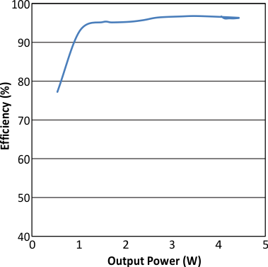 Figure 1. Rectifier Efficiency
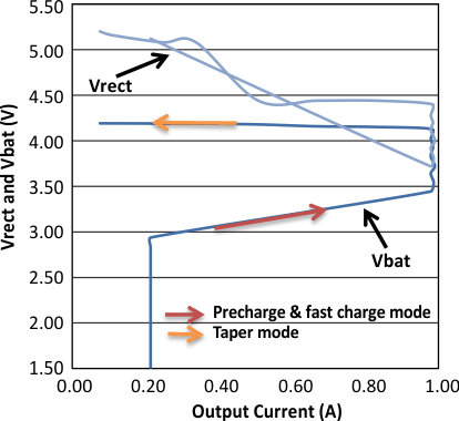 Figure 3. VRECT, VBAT versus Output Current
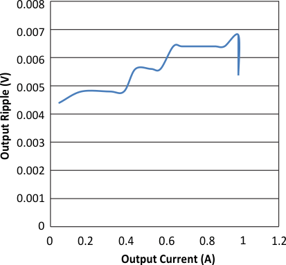 Figure 5. Output Ripple versus Output Current
 Figure 7. bq51052B 300-mA Fast Charge Efficiency (DC Input to DC Output)
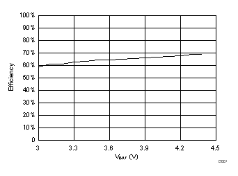 Figure 9. bq51052B 800-mA Fast Charge Efficiency (DC Input to DC Output)
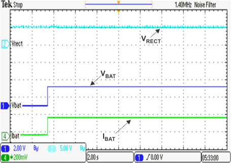 Figure 11. Battery Insertion in Precharge Mode
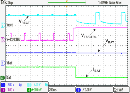 Figure 13. TS Fault
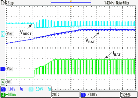 Figure 15. Precharge to Fast-Charge Transition
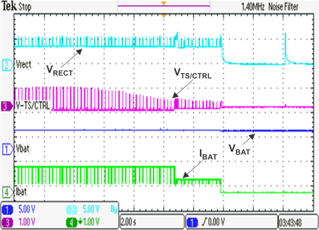 Figure 17. JEITA Functionality (Falling Temp) - bq51050B/bq51051B
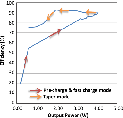 Figure 2. IC Efficiency (AC Input to DC Output)
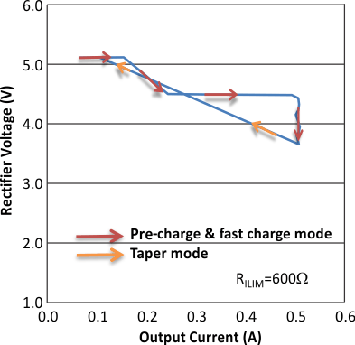 Figure 4. VRECT versus Output Current at RILIM=600 Ω (ILIM = 523 mA)
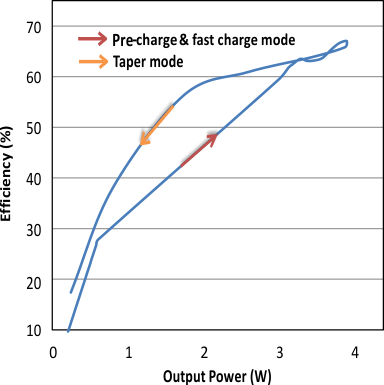 Figure 6. System Efficiency (DC Input to DC Output)
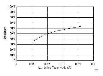 Figure 8. bq51052B 300-mA Taper Charge Efficiency (DC Input to DC Output)
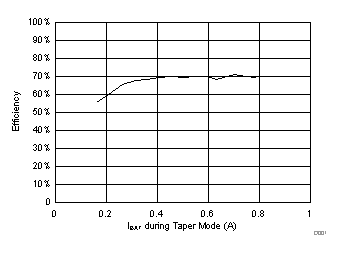 Figure 10. bq51052B 800-mA Taper Charge Efficiency (DC Input to DC Output)
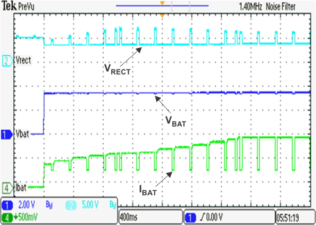 Figure 12. Battery Insertion in Fast-Charge Mode
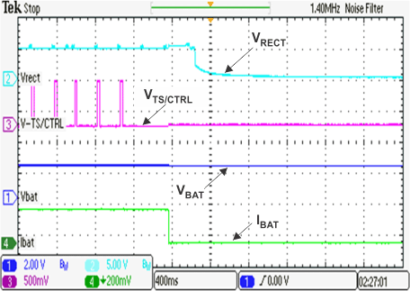 Figure 14. TS Ground Fault
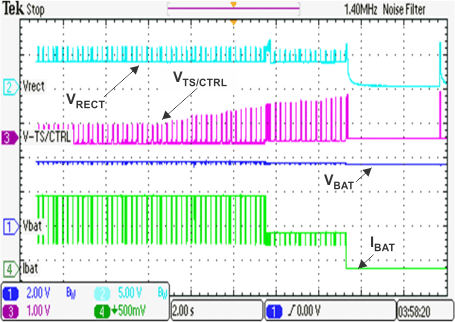 Figure 16. JEITA Functionality (Rising Temp) - bq51050B/bq51051B
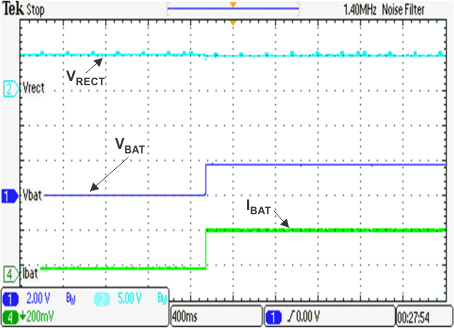 Figure 18. Battery Short to Precharge Mode Transition