SLUSB42F July 2012 – June 2017
PRODUCTION DATA.
- 1 Features
- 2 Applications
- 3 Description
- 4 Revision History
- 5 Device Options
- 6 Pin Configuration and Functions
- 7 Specifications
-
8 Detailed Description
- 8.1 Overview
- 8.2 Functional Block Diagram
- 8.3
Feature Description
- 8.3.1 Using the bq5105x as a Wireless Li-Ion/Li-Pol Battery Charger (With Reference to )
- 8.3.2 Details of a Qi Wireless Power System and bq5105xB Power Transfer Flow Diagrams
- 8.3.3 Battery Charge Profile
- 8.3.4
Battery Charging Process
- 8.3.4.1 Precharge Mode (VBAT ≤ VLOWV)
- 8.3.4.2 Fast Charge Mode / Constant Voltage Mode
- 8.3.4.3 Battery Charge Current Setting Calculations
- 8.3.4.4 Battery-Charger Safety and JEITA Guidelines
- 8.3.4.5 Input Overvoltage
- 8.3.4.6 End Power Transfer Packet (WPC Header 0x02)
- 8.3.4.7 Status Output
- 8.3.4.8 Communication Modulator
- 8.3.4.9 Adaptive Communication Limit
- 8.3.4.10 Synchronous Rectification
- 8.3.4.11 Internal Temperature Sense (TS Function of the TS/CTRL Pin)
- 8.3.4.12 WPC v1.2 Compatibility
- 8.4 Device Functional Modes
- 9 Application and Implementation
- 10Power Supply Recommendations
- 11Layout
- 12Device and Documentation Support
- 13Mechanical, Packaging, and Orderable Information
パッケージ・オプション
デバイスごとのパッケージ図は、PDF版データシートをご参照ください。
メカニカル・データ(パッケージ|ピン)
- RHL|20
- YFP|28
サーマルパッド・メカニカル・データ
- RHL|20
発注情報
9 Application and Implementation
NOTE
Information in the following applications sections is not part of the TI component specification, and TI does not warrant its accuracy or completeness. TI’s customers are responsible for determining suitability of components for their purposes. Customers should validate and test their design implementation to confirm system functionality.
9.1 Application Information
The bq51050B is an integrated wireless power receiver and charger in a single device. The device complies with the WPC v1.2 specifications for a wireless power receiver. When paired with a WPC v1.2 compliant transmitter, it can provide up to 5-W of power for battery charging. There are several tools available for the design of the system. These tools may be obtained by checking the product page at www.ti.com/product/bq51050b.
9.2 Typical Application
9.2.1 bq51050B Used as a Wireless Power Receiver and Li-Ion/Li-Pol Battery Charger
The following application discussion covers the requirements for setting up the bq51050B in a Qi-compliant system for charging a battery.
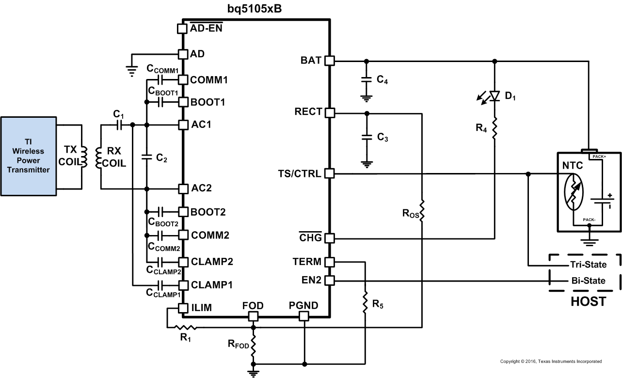 Figure 32. Typical Application Schematic
9.2.1.1 Design Requirements
This application is for a 4.2-V Lithium-Ion battery to be charged at 800 mA. Because this is planned for a WPC v1.2 solution, any of the Qi-certified transmitters can be used interchangeably so no discussion of the TX is required. To charge a 4.20-V Li-Ion battery, the bq51050B will be chosen. Each of the components from the application drawing will be examined. Temperature sensing of the battery must be done with JEITA specifications. An LED indicator is required to notify the user if charging is active.
9.2.1.2 Detailed Design Procedure
9.2.1.2.1 Series and Parallel Resonant Capacitor Selection
Shown in Figure 33, the capacitors C1 (series) and C2 (parallel) make up the dual resonant circuit with the receiver coil. These two capacitors must be sized correctly per the WPC v1.2 specification. Figure 33 shows the equivalent circuit of the dual resonant circuit:
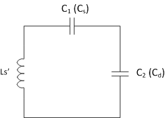 Figure 33. Dual Resonant Circuit with the Receiver Coil
The power receiver design requirements in volume 1 of the WPC v1.2 specification highlights in detail the sizing requirements. To summarize, the receiver designer will be required take inductance measurements with a fixed test fixture. The test fixture is shown in Figure 34:
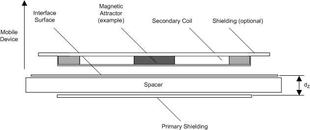 Figure 34. WPC v1.2 Receiver Coil Test Fixture for the Inductance Measurement Ls’
The primary shield is to be 50 mm × 50 mm × 1 mm of Ferrite material PC44 from TDK Corp. The gap (dZ) is to be 3.4 mm. The receiver coil, as it will be placed in the final system (for example, the back cover and battery must be included if the system calls for this), is to be placed on top of this surface and the inductance is to be measured at 1-V RMS and a frequency of 100 kHz. This measurement is termed Ls’. The measurement termed Ls is the free-space inductance. Each capacitor can then be calculated using Equation 6:
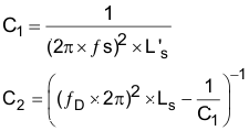
Where fS is 100 kHz +5/–10% and fD is 1 MHz ±10%. C1 must be chosen first prior to calculating C2. The quality factor must be greater than 77 and can be determined by Equation 7:

Where R is the DC resistance of the receiver coil. All other constants are defined above.
For this application, we will design with an inductance measurement (L) of 11 µH and an Ls' of 16 µH with a DC resistance of 191 mΩ. Plugging Ls' into Equation 6 above, we get a value for C1 to be 158.3 nF. The range on the capacitance is about 144 nF to 175 nF. To build the resulting value, the optimum solution is usually found with 3 capacitors in parallel. This allows for more precise selection of values, lower effective resistance and better thermal results. To get 158 nF, choose from standard values. In this case, the values are 68 nF, 47 nF and 39 nF for a total of 154 nF. Well in the required range. Now that C1 is chosen, the value of C2 can be calculated. The result of this calculation is 2.3 nF. The practical solution for this is 2 capacitors, a 2.2 nF capacitor and a 100 pF capacitor. In all cases, these capacitors must have at least a 25-V rating. Solving for the quality factor (Q) this solution shows a rating over 500.
9.2.1.2.2 COMM, CLAMP and BOOT Capacitors
For most applications, the COMM, CLAMP and BOOT capacitors will be chosen to match the Evaluation Module.
The BOOT capacitors are used to allow the internal rectifier FETs to turn on and off properly. These capacitors are on the AC1 or AC2 lines to the Boot nodes and should have a minimum of 10-V rating. A 10-nF capacitor with a 10-V rating is chosen.
The CLAMP capacitors are used to aid the clamping process to protect against overvoltage. Choosing a 0.47-µF capacitor with a 25-V rating is appropriate for most applications.
The COMM capacitors are used to facilitate the communication from the RX to the TX. This selection can vary a bit more than the BOOT and CLAMP capacitors. In general, a 22-nF capacitor is recommended. Based on the results of testing of the communication robustness, a change to a 47-nF capacitor may be in order. The larger the capacitor the larger the deviation will be on the coil which sends a stronger signal to the TX. This also decreases the efficiency somewhat. In this case, choose the 22-nF capacitor with the 25-V rating.
9.2.1.2.3 Charging and Termination Current
The Design Requirements show an 800-mA charging current and an 80-mA termination current.
Setting the charge current (IBULK) is done by selecting the R1 and RFOD. Solving Equation 1 results in RILIM of 393 Ω. Setting RFOD to 200 Ω as a starting point before the FOD calibration is recommended. This leaves 205 Ω for R1. Using standard resistor values (or resistors in series / parallel) can improve accuracy.
Setting the termination current is done with Equation 2. Because 80 mA is 10% of the IBULK (800mA), the RTERM is calculated as (240 * 10) or 2.4 kΩ.
9.2.1.2.4 Adapter Enable
The AD pin will be tied to the external USB power source to allow for an external source to power the system. AD_EN is tied to the gate of Q1 (CSD75205W1015). This allows the bq51050B to sense when power is applied to the AD pin. The EN2 pin controls whether the wired source will be enabled or not. EN2 is tied to the system host to allow it to control the use of the USB power. If wired power is enabled and present, the AD pin will disable the BAT output and then enable Q1 through the AD_EN pin. An external charger is required to take control of the battery charging.
9.2.1.2.5 Charge Indication and Power Capacitors
The CHG pin is open-drain. D1 and R4 are selected as a 2.1-V forward bias capable of 2 mA and a 100-Ω current-limiting resistor.
RECT is used to smooth the internal AC to DC conversion. Two 10-µF capacitors and a 0.1-µF capacitor are chosen. The rating is 25 V.
BAT capacitors are 1.0 µF and 0.1 µF.
9.2.1.3 Application Curves
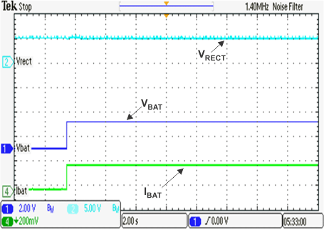 Figure 35. Battery Insertion During Precharge
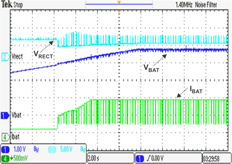 Figure 36. Precharge to Fast-Charge Transition
9.2.2 Application for Wired Charging
The application discussed below will cover the same requirements as the first example and will add a DC supply with a secondary charger. This solution covers using a standard DC supply or a USB port as the supply.
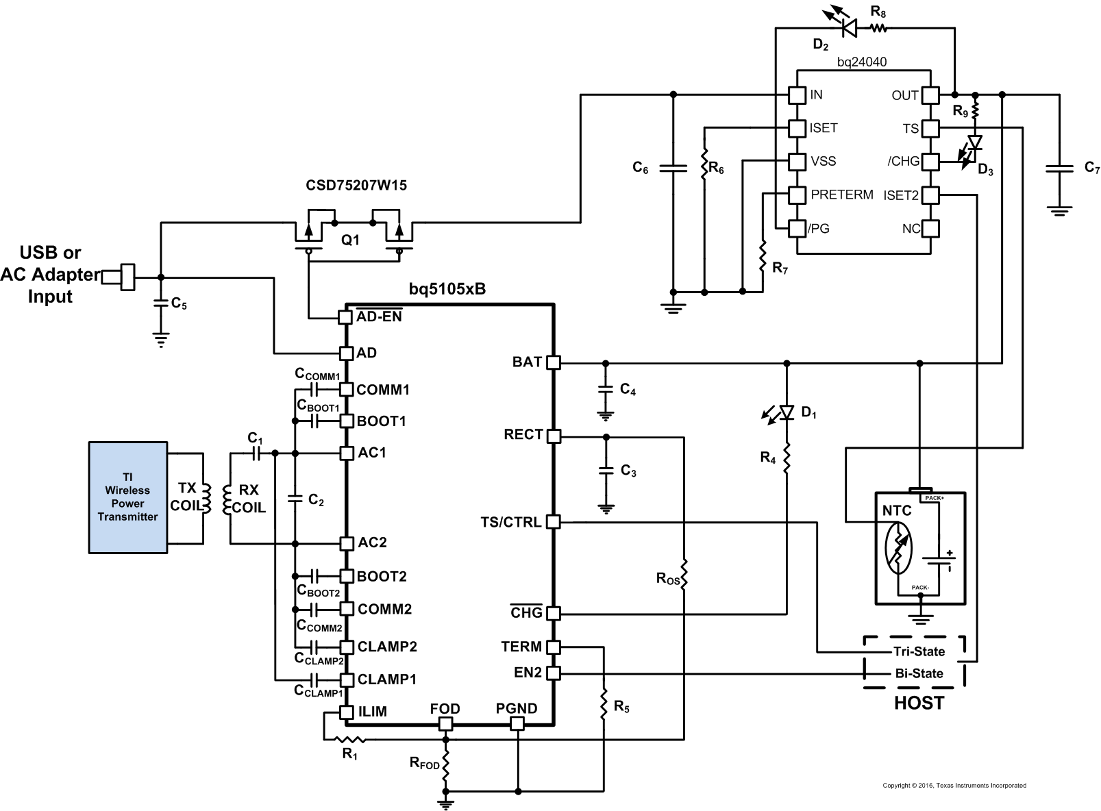 Figure 37. bq51050B Wireless Power Receiver and Wired Charger
9.2.2.1 Design Requirements
The requirements for this solution are identical to the first application so all common components are identical. This solution adds a wired charger and a blocking back-back FET (Q1).
The addition of a wired charger is simply enabled. The AD pin on the bq5105x is tied to the input of the DC supply. When the bq5105x senses a voltage greater than VAD-Pres on the AD pin, the BAT pin will be disabled (high impedance). Once the BAT pin is disabled, the AD_EN pin will transition and enable Q1. If wireless power is not present, the functionality of AD and AD_EN remains and wired charging can take place.
9.2.2.2 Detailed Design Procedure
9.2.2.2.1 Blocking Back-Back FET
Q1 is recommended to eliminate the potential for both wired and wireless systems to drive current to the simultaneously. The charge current and DC voltage level will set up parmerters for the blocking FET. The requirements for this system are 1 A for the wired charger and 5 V DC. The CSD75207W15 is chosen for its low RON and small size.
The wired charger in this solution is the bq24040. See the bq24040 datasheet (SLUS941) for specific component selection.