JAJSMA5C June 2021 – March 2022 BUF802
PRODUCTION DATA
- 1 特長
- 2 アプリケーション
- 3 説明
- 4 Revision History
- 5 Pin Configuration and Functions
- 6 Specifications
- 7 Parameter Measurement Information
- 8 Detailed Description
- 9 Application and Implementation
- 10Power Supply Recommendations
- 11Layout
- 12Device and Documentation Support
- 13Mechanical, Packaging, and Orderable Information
パッケージ・オプション
メカニカル・データ(パッケージ|ピン)
- RGT|16
サーマルパッド・メカニカル・データ
- RGT|16
発注情報
8.4 Device Functional Modes
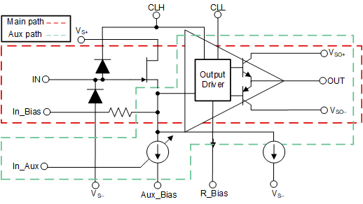
 Figure 8-9 Main Path and Auxiliary
Path
Figure 8-9 Main Path and Auxiliary
PathThe BUF802 has been designed to operate in two modes, Buffer Mode (BF Mode) and Composite Loop Mode (CL Mode):
In BF Mode, the BUF802 uses the JFET, output driver and bipolar transistors in the Main Path to reproduce the signal, applied on IN, at the output of the BUF802. Figure 8-9 shows the Main Path and the Auxiliary Path of the BUF802. The BUF802 can operate from DC to high-frequency and can therefore be used as a standalone buffer. While being used in BF Mode, only the Main Path of the BUF802 is used.
In CL Mode, the BUF802 utilizes the Auxiliary signal path and the Main Path to control the output voltage. As the name suggests in the Composite Loop Mode, the BUF802 is used in a composite loop with a precision amplifier to achieve DC precision and a wide, large-signal bandwidth simultaneously. The composite loop splits the applied signal to low-frequency and high-frequency components and passes them over to different circuits with suitable transfer function. The low-frequency and high-frequency signal components then recombine inside the BUF802 and are repoduced at the OUT pin.