JAJSK09B November   2014  – September 2020 CC3100MOD

PRODUCTION DATA  

  1. 特長
  2. アプリケーション
  3. 概要
  4. 機能ブロック図
  5. 機能ブロック図
  6. Revision History
  7. Terminal Configuration and Functions
    1. 7.1 CC3100MOD Pin Diagram
    2. 7.2 Pin Attributes
      1.      10
  8. Specifications
    1. 8.1  Absolute Maximum Ratings
    2. 8.2  ESD Ratings
    3. 8.3  Power-On Hours (POH)
    4. 8.4  Recommended Operating Conditions
    5. 8.5  Power Consumption Summary
    6. 8.6  TX Power and IBAT versus TX Power Level Settings
    7. 8.7  Brownout and Blackout Conditions
    8. 8.8  Electrical Characteristics (3.3 V, 25°C)
    9. 8.9  WLAN RF Characteristics
      1. 8.9.1 WLAN Receiver Characteristics
      2. 8.9.2 WLAN Transmitter Characteristics
    10. 8.10 Reset Requirement
    11. 8.11 Thermal Resistance Characteristics for MOB Package
    12. 8.12 Timing and Switching Characteristics
      1. 8.12.1 Wake-Up Sequence
      2. 8.12.2 Wake Up From Hibernate
        1. 8.12.2.1 nHIB Timing Requirements #GUID-400CF46C-B651-457D-A1D7-C5F78DD51018/SWRS1661423
      3. 8.12.3 Interfaces
        1. 8.12.3.1 Host SPI Interface Timing
        2. 8.12.3.2 SPI Host Interface
    13. 8.13 Host UART
      1. 8.13.1 5-Wire UART Topology
      2. 8.13.2 4-Wire UART Topology
      3. 8.13.3 3-Wire UART Topology
  9. Detailed Description
    1. 9.1 Overview
    2. 9.2 Module Features
      1. 9.2.1 WLAN
      2. 9.2.2 Network Stack
      3. 9.2.3 Host Interface and Driver
      4. 9.2.4 System
    3. 9.3 Functional Block Diagram
    4. 9.4 Wi-Fi Network Processor Subsystem
    5. 9.5 Power-Management Subsystem
      1. 9.5.1 VBAT Wide-Voltage Connection
    6. 9.6 Low-Power Operating Modes
      1. 9.6.1 Low-Power Deep Sleep
      2. 9.6.2 Hibernate
  10. 10Applications, Implementation, and Layout
    1. 10.1 Reference Schematics
    2. 10.2 Design Requirements
    3. 10.3 Layout Recommendations
      1. 10.3.1 RF Section (Placement and Routing)
      2. 10.3.2 Antenna Placement and Routing
      3. 10.3.3 Transmission Line Considerations
  11. 11Environmental Requirements and Specifications
    1. 11.1 Temperature
      1. 11.1.1 PCB Bending
    2. 11.2 Handling Environment
      1. 11.2.1 Terminals
      2. 11.2.2 Falling
    3. 11.3 Storage Condition
      1. 11.3.1 Moisture Barrier Bag Before Opened
      2. 11.3.2 Moisture Barrier Bag Open
    4. 11.4 Baking Conditions
    5. 11.5 Soldering and Reflow Condition
  12. 12Device and Documentation Support
    1. 12.1 Device Support
      1. 12.1.1 Development Support
        1. 12.1.1.1 Firmware Updates
      2. 12.1.2 Device Nomenclature
    2. 12.2 Documentation Support
    3. 12.3 Trademarks
    4. 12.4 静電気放電に関する注意事項
    5. 12.5 用語集
  13. 13Mechanical, Packaging, and Orderable Information
    1. 13.1 Mechanical Drawing
    2. 13.2 Package Option
      1. 13.2.1 Packaging Information
      2. 13.2.2 Tape and Reel Information

パッケージ・オプション

デバイスごとのパッケージ図は、PDF版データシートをご参照ください。

メカニカル・データ(パッケージ|ピン)
  • MOB|63
サーマルパッド・メカニカル・データ
発注情報

SPI Host Interface

The device interfaces to an external host using the SPI. The CC3100 device can interrupt the host using the HOST_INTR line to initiate the data transfer over the interface. The SPI host interface can work up to a speed of 20 MHz.

Figure 8-9 shows the SPI host interface.
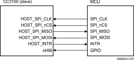
GUID-1EB772FE-D86C-40AE-869D-E97C23FFBB2D-low.gifFigure 8-9 SPI Host Interface

Table 8-3 lists the SPI host interface pins.

Table 8-3 SPI Host Interface
PIN NAMEDESCRIPTION
HOST_SPI_CLKClock (up to 20 MHz) from MCU host to CC3100 device
HOST_SPI_nCSCS (active low) signal from MCU host to CC3100 device
HOST_SPI_MOSIData from MCU host to CC3100 device
HOST_INTRInterrupt from CC3100 device to MCU host
HOST_SPI_MISOData from CC3100 device to MCU host
nHIBActive-low signal that commands the CC3100 device to enter hibernate mode (lowest power state)