JAJSGW3D April   2019  – May 2021 CC3235S , CC3235SF

PRODUCTION DATA  

  1. 特長
  2. アプリケーション
  3. 概要
  4. 機能ブロック図
  5. Revision History
  6. Device Comparison
    1. 6.1 Related Products
  7. Terminal Configuration and Functions
    1. 7.1 Pin Diagram
    2. 7.2 Pin Attributes
      1.      11
    3. 7.3 Signal Descriptions
      1.      13
    4. 7.4 Pin Multiplexing
    5. 7.5 Drive Strength and Reset States for Analog and Digital Multiplexed Pins
    6. 7.6 Pad State After Application of Power to Device, Before Reset Release
    7. 7.7 Connections for Unused Pins
  8. Specifications
    1. 8.1  Absolute Maximum Ratings
    2. 8.2  ESD Ratings
    3. 8.3  Power-On Hours (POH)
    4. 8.4  Recommended Operating Conditions
    5. 8.5  Current Consumption Summary (CC3235S)
      1.      24
      2.      25
    6. 8.6  Current Consumption Summary (CC3235SF)
      1.      27
      2.      28
    7. 8.7  TX Power Control for 2.4 GHz Band
    8. 8.8  TX Power Control for 5 GHz
    9. 8.9  Brownout and Blackout Conditions
    10. 8.10 Electrical Characteristics for GPIO Pins
      1.      33
      2.      34
    11. 8.11 Electrical Characteristics for Pin Internal Pullup and Pulldown
    12. 8.12 WLAN Receiver Characteristics
      1.      37
      2.      38
    13. 8.13 WLAN Transmitter Characteristics
      1.      40
      2.      41
    14. 8.14 WLAN Transmitter Out-of-Band Emissions
      1.      43
      2.      44
    15. 8.15 BLE/2.4 GHz Radio Coexistence and WLAN Coexistence Requirements
    16. 8.16 Thermal Resistance Characteristics for RGK Package
    17. 8.17 Timing and Switching Characteristics
      1. 8.17.1 Power Supply Sequencing
      2. 8.17.2 Device Reset
      3. 8.17.3 Reset Timing
        1. 8.17.3.1 nRESET (32-kHz Crystal)
        2.       52
        3.       53
        4. 8.17.3.2 nRESET (External 32-kHz Clock)
          1.        55
      4. 8.17.4 Wakeup From HIBERNATE Mode
      5. 8.17.5 Clock Specifications
        1. 8.17.5.1 Slow Clock Using Internal Oscillator
        2. 8.17.5.2 Slow Clock Using an External Clock
          1.        60
        3. 8.17.5.3 Fast Clock (Fref) Using an External Crystal
          1.        62
        4. 8.17.5.4 Fast Clock (Fref) Using an External Oscillator
          1.        64
      6. 8.17.6 Peripherals Timing
        1. 8.17.6.1  SPI
          1. 8.17.6.1.1 SPI Master
            1.         68
          2. 8.17.6.1.2 SPI Slave
            1.         70
        2. 8.17.6.2  I2S
          1. 8.17.6.2.1 I2S Transmit Mode
            1.         73
          2. 8.17.6.2.2 I2S Receive Mode
            1.         75
        3. 8.17.6.3  GPIOs
          1. 8.17.6.3.1 GPIO Output Transition Time Parameters (Vsupply = 3.3 V)
            1.         78
          2. 8.17.6.3.2 GPIO Input Transition Time Parameters
            1.         80
        4. 8.17.6.4  I2C
          1.        82
        5. 8.17.6.5  IEEE 1149.1 JTAG
          1.        84
        6. 8.17.6.6  ADC
          1.        86
        7. 8.17.6.7  Camera Parallel Port
          1.        88
        8. 8.17.6.8  UART
        9. 8.17.6.9  SD Host
        10. 8.17.6.10 Timers
  9. Detailed Description
    1. 9.1  Overview
    2. 9.2  Arm® Cortex®-M4 Processor Core Subsystem
    3. 9.3  Wi-Fi® Network Processor Subsystem
      1. 9.3.1 WLAN
      2. 9.3.2 Network Stack
    4. 9.4  Security
    5. 9.5  FIPS 140-2 Level 1 Certification
    6. 9.6  Power-Management Subsystem
    7. 9.7  Low-Power Operating Mode
    8. 9.8  Memory
      1. 9.8.1 External Memory Requirements
      2. 9.8.2 Internal Memory
        1. 9.8.2.1 SRAM
        2. 9.8.2.2 ROM
        3. 9.8.2.3 Flash Memory
        4. 9.8.2.4 Memory Map
    9. 9.9  Restoring Factory Default Configuration
    10. 9.10 Boot Modes
      1. 9.10.1 Boot Mode List
    11. 9.11 Hostless Mode
  10. 10Applications, Implementation, and Layout
    1. 10.1 Application Information
      1. 10.1.1 BLE/2.4 GHz Radio Coexistence
      2. 10.1.2 Antenna Selection
      3. 10.1.3 Typical Application
    2. 10.2 PCB Layout Guidelines
      1. 10.2.1 General PCB Guidelines
      2. 10.2.2 Power Layout and Routing
        1. 10.2.2.1 Design Considerations
      3. 10.2.3 Clock Interface Guidelines
      4. 10.2.4 Digital Input and Output Guidelines
      5. 10.2.5 RF Interface Guidelines
  11. 11Device and Documentation Support
    1. 11.1  Third-Party Products Disclaimer
    2. 11.2  Tools and Software
    3. 11.3  Firmware Updates
    4. 11.4  Device Nomenclature
    5. 11.5  Documentation Support
    6. 11.6  Related Links
    7. 11.7  サポート・リソース
    8. 11.8  Trademarks
    9. 11.9  Electrostatic Discharge Caution
    10. 11.10 Export Control Notice
    11. 11.11 Glossary
  12. 12Mechanical, Packaging, and Orderable Information
    1. 12.1 Packaging Information
      1. 12.1.1 Package Option Addendum
        1. 12.1.1.1 Packaging Information
        2. 12.1.1.2 Tape and Reel Information

パッケージ・オプション

メカニカル・データ(パッケージ|ピン)
サーマルパッド・メカニカル・データ
発注情報

機能ブロック図

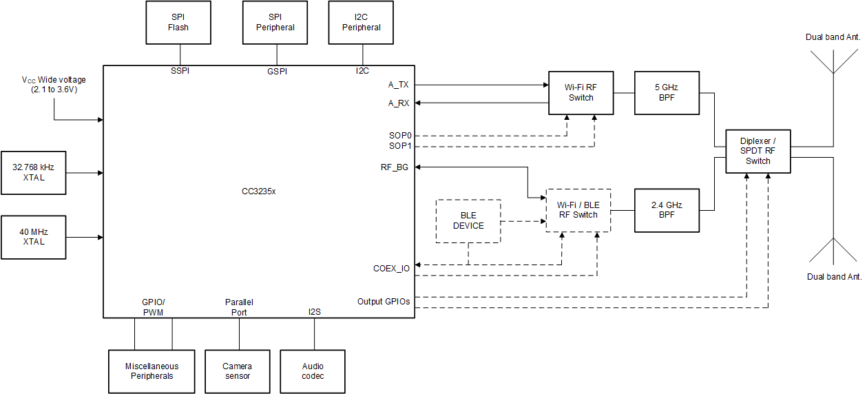
図 4-1 に、CC3235x SimpleLink™ Wi-Fi® ソリューションの機能ブロック図を示します。

GUID-538C971C-A5B4-4B0D-86C6-717A3E6AAABA-low.gif
注:ダイプレクサは、信号アンテナ・ソリューションに使用されます。アンテナ選択機能 (デュアル・アンテナ) を使用する場合、ダイプレクサの後ろに SPDT スイッチと 2 つの GPIO ラインが必要です。
図 4-1 機能ブロック図

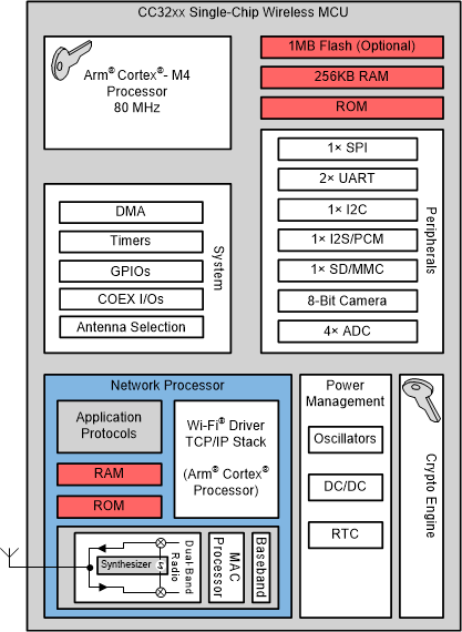
CC3235x デバイスのハードウェア概要を 図 4-2 に示します。

GUID-C1B7F494-6A4D-4172-90D9-1F5106DAA414-low.gif図 4-2 CC3235x ハードウェアの概要

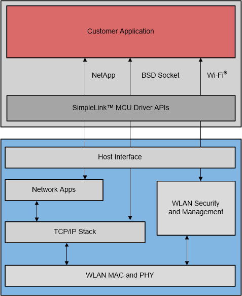
CC3235x デバイスの組み込みソフトウェアの概要を 図 4-3 に示します。

GUID-E0370FE7-0B85-4C84-AA71-1F08B5314159-low.gif図 4-3 CC3235x 組み込みソフトウェアの概要