SLLSEL1 November   2014 CDCL1810A

PRODUCTION DATA.  

  1. Features
  2. Applications
  3. Description
  4. Simplified Schematic
  5. Revision History
  6. Device Comparison Tables
  7. Pin Configuration and Functions
  8. Specifications
    1. 8.1 Absolute Maximum Ratings
    2. 8.2 Handling Ratings
    3. 8.3 Recommended Operating Conditions
    4. 8.4 Thermal Information
    5. 8.5 DC Electrical Characteristics
    6. 8.6 AC Electrical Characteristics
    7. 8.7 AC Electrical Characteristics for the SDA/SCL Interface
    8. 8.8 Typical Characteristics
  9. Detailed Description
    1. 9.1 Overview
    2. 9.2 Functional Block Diagram
    3. 9.3 Feature Description
      1. 9.3.1 Output Enable/Disable
      2. 9.3.2 SDA/SCL Interface
        1. 9.3.2.1 SDA/SCL Bus Slave Device Address
        2. 9.3.2.2 SDA/SCL Connections Recommendations
    4. 9.4 Device Functional Modes
    5. 9.5 Programming
      1. 9.5.1 SDA/SCL Interface
      2. 9.5.2 Command Code Definition
      3. 9.5.3 SDA/SCL Timing Characteristics
      4. 9.5.4 SDA/SCL Programming Sequence
    6. 9.6 Register Maps
      1. 9.6.1 SDA/SCL Bus Configuration Command Bitmap
        1. 9.6.1.1 Byte 0:
        2. 9.6.1.2 Byte 1:
        3. 9.6.1.3 Byte 2:
        4. 9.6.1.4 Byte 3:
        5. 9.6.1.5 Byte 4:
        6. 9.6.1.6 Byte 5:
        7. 9.6.1.7 Byte 6:
  10. 10Application and Implementation
    1. 10.1 Application Information
      1. 10.1.1 Clock Distribution for Multiple TI Keystone DSPs
        1. 10.1.1.1 Design Requirements
        2. 10.1.1.2 Detailed Design Procedure
        3. 10.1.1.3 Application Curves
  11. 11Power Supply Recommendations
  12. 12Layout
    1. 12.1 Layout Guidelines
    2. 12.2 Layout Example
  13. 13Device and Documentation Support
    1. 13.1 Trademarks
    2. 13.2 Electrostatic Discharge Caution
    3. 13.3 Glossary
  14. 14Mechanical, Packaging, and Orderable Information
    1. 12.1 Trademarks
    2. 12.2 Electrostatic Discharge Caution
    3. 12.3 Glossary
  15. 13Mechanical, Packaging, and Orderable Information

パッケージ・オプション

メカニカル・データ(パッケージ|ピン)
サーマルパッド・メカニカル・データ
発注情報

12 Layout

12.1 Layout Guidelines

  • Keep the connections between the bypass capacitors and the power supply on the device as short as possible.
  • Ground the other side of the capacitor using a low impedance connection to the ground plane.
  • If the capacitors are mounted on the back side, 0402 components can be employed; however, soldering to the Thermal Dissipation Pad can be difficult.
  • For component side mounting, use 0201 body size capacitors to facilitate signal routing.

NOTE

The device must be soldered to ground (VSS) using as many ground vias as possible. The device performance will be severely impacted if the exposed thermal pad is not grounded appropriately.

12.2 Layout Example

laoyoutTOP.png
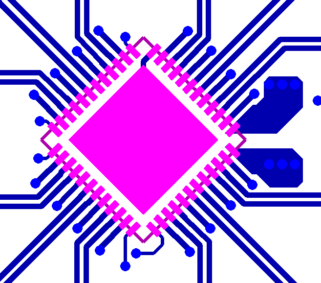
Figure 12. Layout Example: Signal Layer (TOP)
laoyoutBOTTOM.png
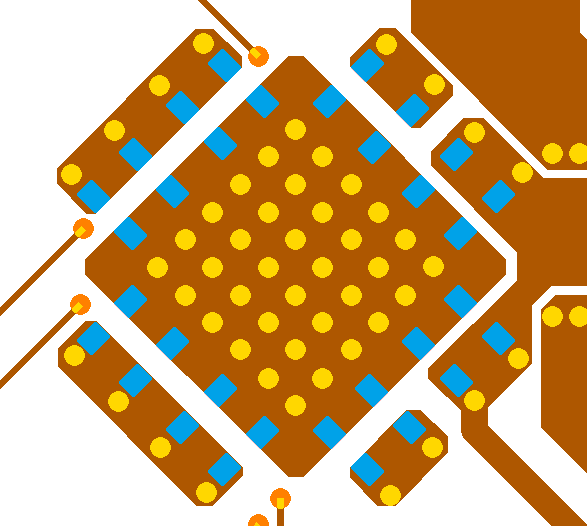
Figure 13. Layout Example: Bottom Layer with Decoupling Capacitors