JAJSEH8C December   2006  – January 2018 DAC8560

PRODUCTION DATA.  

  1. 特長
  2. アプリケーション
  3. 概要
    1.     Device Images
      1.      機能ブロック図
  4. 改訂履歴
  5. 概要(続き)
  6. Pin Configuration and Functions
    1.     Pin Functions
  7. Specifications
    1. 7.1  Absolute Maximum Ratings
    2. 7.2  ESD Ratings
    3. 7.3  Recommended Operating Conditions
    4. 7.4  Thermal Information
    5. 7.5  Electrical Characteristics
    6. 7.6  Timing Requirements
    7. 7.7  Typical Characteristics: Internal Reference
    8. 7.8  Typical Characteristics: DAC at VDD = 5 V
    9. 7.9  Typical Characteristics: DAC at VDD = 3.6 V
    10. 7.10 Typical Characteristics: DAC at VDD = 2.7 V
  8. Detailed Description
    1. 8.1 Overview
    2. 8.2 Functional Block Diagram
    3. 8.3 Feature Description
      1. 8.3.1 Digital-to-Analog Converter (DAC)
      2. 8.3.2 Resistor String
      3. 8.3.3 Output Amplifier
      4. 8.3.4 DAC Noise Performance
      5. 8.3.5 Internal Reference
        1. 8.3.5.1 Enable/Disable Internal Reference
        2. 8.3.5.2 Internal Reference Load
          1. 8.3.5.2.1 Supply Voltage
          2. 8.3.5.2.2 Temperature Drift
          3. 8.3.5.2.3 Noise Performance
          4. 8.3.5.2.4 Load Regulation
          5. 8.3.5.2.5 Long-Term Stability
          6. 8.3.5.2.6 Thermal Hysteresis
    4. 8.4 Device Functional Modes
      1. 8.4.1 Power-Down Modes
    5. 8.5 Programming
      1. 8.5.1 Serial Interface
      2. 8.5.2 Input Shift Register
      3. 8.5.3 SYNC Interrupt
      4. 8.5.4 Power-On Reset
    6. 8.6 Register Maps
      1. 8.6.1 Write Sequence for Disabling the DAC8560 Internal Reference
        1. Table 1. Write Sequence for Disabling the DAC8560 Internal Reference
      2. 8.6.2 Enabling the DAC8560 Internal Reference (Write Sequence 1 of 2)
        1. Table 2. Enabling the DAC8560 Internal Reference (Write Sequence 1 of 2)
      3. 8.6.3 Enabling the DAC8560 Internal Reference (Write Sequence 2 of 2)
        1. Table 3. Enabling the DAC8560 Internal Reference (Write Sequence 2 of 2)
      4. 8.6.4 DAC8560 Data Input Register Format
        1. Table 4. DAC8560 Data Input Register Format
  9. Application and Implementation
    1. 9.1 Application Information
    2. 9.2 Typical Applications
      1. 9.2.1 Design Requirements
      2. 9.2.2 Detailed Design Procedure or Bipolar Operation > ±VREF
        1. 9.2.2.1 Bipolar Operation Greater Than ±VREF
          1. 9.2.2.1.1 Passive Component Selection
          2. 9.2.2.1.2 Amplifier Selection
        2. 9.2.2.2 Microprocessor Interfacing
          1. 9.2.2.2.1 DAC8560 to 8051 Interface
          2. 9.2.2.2.2 DAC8560 to Microwire Interface
          3. 9.2.2.2.3 DAC8560 to 68HC11 Interface
      3. 9.2.3 Application Curves
  10. 10Power Supply Recommendations
  11. 11Layout
    1. 11.1 Layout Guidelines
    2. 11.2 Layout Example
  12. 12デバイスおよびドキュメントのサポート
    1. 12.1 ドキュメントのサポート
      1. 12.1.1 関連資料
    2. 12.2 ドキュメントの更新通知を受け取る方法
    3. 12.3 コミュニティ・リソース
    4. 12.4 商標
    5. 12.5 静電気放電に関する注意事項
    6. 12.6 Glossary
  13. 13メカニカル、パッケージ、および注文情報

パッケージ・オプション

メカニカル・データ(パッケージ|ピン)
サーマルパッド・メカニカル・データ
発注情報

Typical Characteristics: Internal Reference

At TA = 25°C, unless otherwise noted.
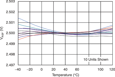
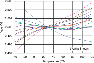
DAC8560 tc_vref-tmp_cd_las464.gif
Figure 2. Internal Reference Voltage vs Temperature (Grades C and D)
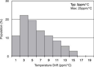
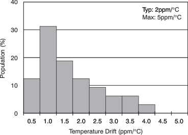
DAC8560 tc_tmp_drift_cd_40_las464.gif
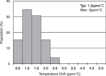
Figure 4. Reference Output Temperature Drift (–40°C to 120°C, Grades C and D)
DAC8560 tc_tmp_drift_cd_0_las464.gif
Figure 6. Reference Output Temperature Drift (0°C to 120°C, Grades C and D)
DAC8560 tc_ref_noise-freq_las464.gif
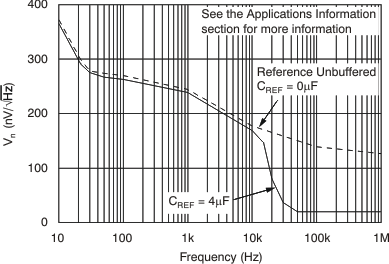
Explained in more detail in Application and Implementation.
Figure 8. Internal Reference Noise Density vs Frequency
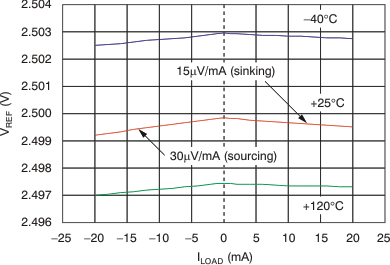
DAC8560 tc_vref-iload_cd_las464.gif
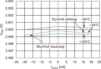
Figure 10. Internal Reference Voltage vs Load Current (Grades C and D)
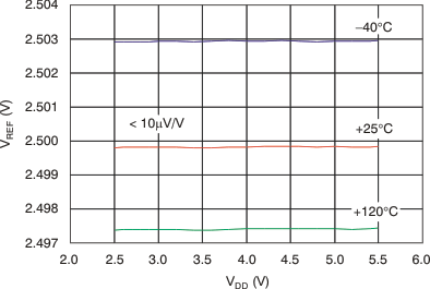
DAC8560 tc_vref-vdd_cd_las464.gif
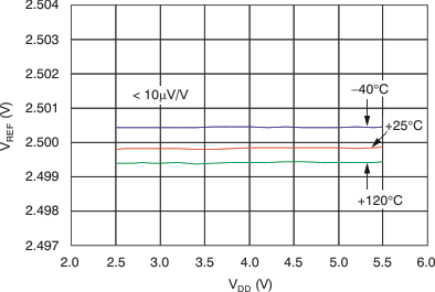
Figure 12. Internal Reference Voltage vs Supply Voltage (Grades C and D)
DAC8560 tc_vref-tmp_ab_las464.gif
Figure 3. Internal Reference Voltage vs Temperature (Grades A and B)
DAC8560 tc_temp_drift_ab_las464.gif
Figure 5. Reference Output Temperature Drift (–40°C to 120°, Grades A and B)
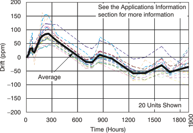
DAC8560 tc_long_term_drift_las464.gif
Explained in more detail in Application and Implementation .
Figure 7. Long-Term Stability/Drift (1)
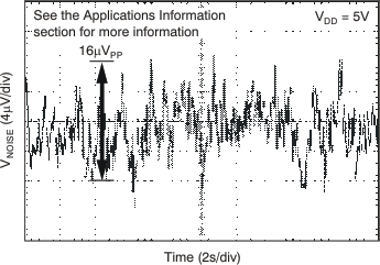
DAC8560 tc_int_ref_noise_las464.gif
Explained in more detail in Application and Implementation.
Figure 9. Internal Reference Noise 0.1 Hz to 10 Hz
DAC8560 tc_vref-iload_ab_las464.gif
Figure 11. Internal Reference Voltage vs Load Current (Grades A and B)
DAC8560 tc_vref-vdd_ab_las464.gif
Figure 13. Internal Reference Voltage vs Supply Voltage (Grades A and B)