SLWS237A November 2012 – November 2014 DRV11873
PRODUCTION DATA.
- 1 Features
- 2 Applications
- 3 Description
- 4 Simplified Schematic
- 5 Revision History
- 6 Pin Configuration and Functions
- 7 Specifications
- 8 Detailed Description
- 9 Application and Implementation
- 10Power Supply Recommendations
- 11Layout
- 12Device and Documentation Support
- 13Mechanical, Packaging, and Orderable Information
8 Detailed Description
8.1 Overview
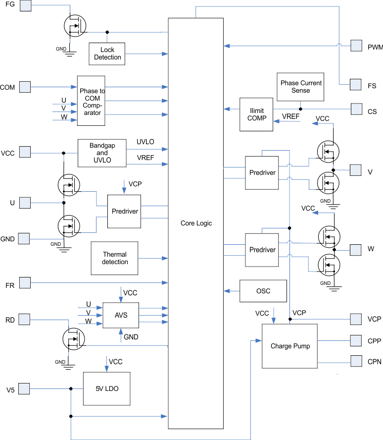
DRV11873 is a three-phase, sensorless motor driver with integrated power MOSFETs with drive current capability up to 1.5-A continuous and 2-A peak. It is specifically designed for fan motor drive applications with low noise and low external component count. DRV11873 has built-in overcurrent protection with no external current sense resistor needed. The synchronous rectification mode of operation achieves increased efficiency for motor driver applications. A 5-V LDO is available to provide up to 20 mA to an external load. DRV11873 outputs FG and RD to indicate motor status with open-drain output. A 150° sensorless BEMF control scheme was implemented for a three-phase motor. DRV11873 can fit a wide range of fan motors with the FS pin selection function. Motor speed can be controlled by adjusting VCC or providing a PWM input. Voltage surge protection scheme prevents the input VCC capacitor from overcharge during motor braking mode. DRV11873 has multiple built-in protection blocks including UVLO, overcurrent protection, lock protection, and thermal shutdown protection.
8.2 Functional Block Diagram
8.3 Feature Description
8.3.1 Speed Control
DRV11873 can control motor speed through either the PWMIN or VCC pin. Motor speed increases with higher PWMIN duty cycle or VCC input voltage. The curve of motor speed (RPM) vs PWMIN duty cycle or VCC input voltage is close to linear in most cases. However, motor characteristics affect the linearity of this speed curve. DRV11873 can operate at low VCC input voltage ≥ 4.1 V. The PWMIN pin is pulled up to V5 internally and the frequency range can vary from 7 to 100 kHz. The motor driver MOSFETs operate at a constant switching frequency of 125 kHz when the FS pin is pulled high and 62.5 kHz when the FS pin is pulled low. With this high switching frequency, DRV11873 can eliminate audible noise and reduce the ripple of VCC input voltage and current.
8.3.2 Frequency Generator
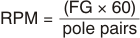
The FG output is a 50% duty square wave output in the normal operation condition. Its frequency represents the motor speed and phase information. The FG pin is an open-drain output. An external pullup resistor is needed to connect any external system. During the start up, the FG output remains at high impedance until the motor speed reaches a certain level and BEMF is detected. If FG is not used, this pin can be left floating. The FG pin can be tied to either V5 or VCC through a pullup resistor. Normally, the pullup resistor value can be 100 kΩ or higher. During lock protection, the FG output remains high until the lockout protection is dismissed and restart is completed. A current limit function is built in for the FG pin which prevents the open-drain MOSFET from damage if VCC or V5 is accidentally connected to the FG pin. To calculate RPM based on FG frequency, refer to Equation 1.
where
- FG is in hertz (Hz)
8.3.3 FS Setting
DRV11873 can fit a wide range of fan motors by setting the FS pin. For high speed fan motors with low motor winding resistance and low inductance, the FS pin should be pulled high. For low speed fan motors with high motor winding resistance and high inductance, the FS pin should be pulled low. Through FS pin selection, DRV11873 can be used for wide applications from low-speed refrigerator cooling fans to high-speed server cooling fans. FS status can only be set during device power up.
8.3.4 Lock Protection and RD Output
If the motor is blocked or stopped by an external force, the lock protection will be triggered after detection time. During lock detection time, the circuit monitors the FG signal. If the FG output does not change state during the lock detection time, the lock protection will stop driving the motor. After lock release time, DRV11873 resumes driving the motor. If the lock condition is still present, DRV11873 proceeds with the next lock protection cycle until the lock condition is removed. With this lock protection, the motor and device do not get overheated or damaged. A different FS setting determines a different lock detection and lock release time. See the Electrical Characteristics for the different lock detection and release times.
The RD pin is an open-drain output which can be tied to either V5 or VCC through a pullup resistor. Normally, the pullup resistor value can be 100 kΩ or higher. During the lock protection condition, the RD output remains high until the lock protection is dismissed and restart is completed. A current limit function is built in for the RD pin which prevents the open-drain MOSFET from damage if VCC or V5 is accidentally connected to the RD pin.
8.3.5 Reverse Spin Control FR
DRV11873 has an FR pin to set the motor for forward or reverse spin. During DRV11873 power up, FR status is set. During normal operation, the spin direction of the motor does not change if the FR status is changed. The FR status can be reset if the PWMIN is pulled low; if FS is high, PWM must be pulled low for 300 µs, and if FS is low, PWM must be low for 600 µs. After being pulled down for the appropriate time, the FR status resets upon the PWM rising edge.
8.3.6 5-V LDO
DRV11873 has a built-in 5-V LDO which can output a 20-mA load current. It can provide 5-V bias voltage for external use. TI recommends a 2.2-µF ceramic capacitor to connect closely on the PCB layout between the V5 pin and ground.
8.3.7 Overcurrent Protection
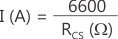
DRV11873 can adjust overcurrent through the external resistor connected to the CS pin and ground. Without using an external current sense resistor, DRV11873 senses the current through the power MOSFET. Therefore, no power loss occurs during the current sensing. This current sense architecture improves the system efficiency. Shorting the CS pin to ground disables overcurrent protection. During overcurrent protection, DRV11873 only limits the current to the motor and it does not shut down the operation. The overcurrent threshold can be set by the value of the external resistor through Equation 2.
During motor start up, the overcurrent level is increased to 1.5 times the value set by RCS. If the overcurrent protection is triggered during the start up sequence, the motor will fail to start.
8.3.8 UVLO
DRV11873 has a built-in UVLO function block. The hysteresis of the UVLO threshold is 200 mV. The device is locked out when VCC reaches 4.1 V and woken up at 4.3 V.
8.3.9 Thermal Shutdown
DRV11873 has a built-in thermal shutdown function, which shuts down the device when the junction temperature is over 160°C and resumes operating when the junction temperature drops back to 150°C.
8.3.10 Anti-Voltage Surge (AVS)
The DRV11873 has a protection feature to prevent any energy from returning to the power supply when the motor is braked. This feature, AVS, protects the device as well as any other device from allowing VCC from increasing. AVS works when the motor is braked to a lower speed and when the motor is stopped.
8.4 Device Functional Modes
8.4.1 Startup
At startup, commutation logic starts to drive the motor with one phase high, one phase low, and the third shut off. If a zero-cross is detected on the shut off phase, commutation logic advances to the next step; the same phase high, the shut off phase goes low, and the low phase is shut off. Initially, the BEMF is not strong enough to detect the zero crossings, at this very initial stage the commutation switches automatically until the BEMF is large enough to read. In startup mode, 100% duty cycle is applied regardless of PWM input. After the commutation logic receives 4 continuous successful zero-crossings, it switches to normal operation.
In certain cases, the motor may have initial speed when the device attempts to startup the motor again. When this occurs, the commutation logic jumps over the startup process and goes to normal operation directly.
8.4.2 Closed Loop Control
After the motor is started successfully, the start up control switches to steady state operation. In steady state control, the motor is commutated 150°. This is an advanced trapezoidal method that allows the device to drive the phases gradually to the maximum current and gradually to 0 at commutation.
8.4.3 AVS Protection
When the device is commanded to decelerate or stop the motor, in order to protect the IC and the system, the DRV11873 has AVS protection. This function keeps the voltage supply, VCC, from surging above the nominal value. To do this, the device monitors the current flow in the MOSFETs and is able to sense when the surging starts to occur. The AVS function controls the current, not allowing it to charge back to VCC so that there is no voltage surging.