SLWS237A November   2012  – November 2014 DRV11873

PRODUCTION DATA.  

  1. Features
  2. Applications
  3. Description
  4. Simplified Schematic
  5. Revision History
  6. Pin Configuration and Functions
  7. Specifications
    1. 7.1 Absolute Maximum Ratings
    2. 7.2 Handling Ratings
    3. 7.3 Recommended Operating Conditions
    4. 7.4 Thermal Information
    5. 7.5 Electrical Characteristics
    6. 7.6 Typical Characteristics
  8. Detailed Description
    1. 8.1 Overview
    2. 8.2 Functional Block Diagram
    3. 8.3 Feature Description
      1. 8.3.1  Speed Control
      2. 8.3.2  Frequency Generator
      3. 8.3.3  FS Setting
      4. 8.3.4  Lock Protection and RD Output
      5. 8.3.5  Reverse Spin Control FR
      6. 8.3.6  5-V LDO
      7. 8.3.7  Overcurrent Protection
      8. 8.3.8  UVLO
      9. 8.3.9  Thermal Shutdown
      10. 8.3.10 Anti-Voltage Surge (AVS)
    4. 8.4 Device Functional Modes
      1. 8.4.1 Startup
      2. 8.4.2 Closed Loop Control
      3. 8.4.3 AVS Protection
  9. Application and Implementation
    1. 9.1 Application Information
    2. 9.2 Typical Application
      1. 9.2.1 Design Requirements
      2. 9.2.2 Detailed Design Procedure
      3. 9.2.3 Application Curves
  10. 10Power Supply Recommendations
  11. 11Layout
    1. 11.1 Layout Guidelines
    2. 11.2 Layout Example
  12. 12Device and Documentation Support
    1. 12.1 Trademarks
    2. 12.2 Electrostatic Discharge Caution
    3. 12.3 Glossary
  13. 13Mechanical, Packaging, and Orderable Information

パッケージ・オプション

メカニカル・データ(パッケージ|ピン)
サーマルパッド・メカニカル・データ
発注情報

11 Layout

11.1 Layout Guidelines

  • Place VCC, GND, U, V, and W pins with thick traces because high current passes through these traces.
  • Place the 10-μF capacitor between VCC and GND, and as close to the VCC and GND pins as possible.
  • Place the capacitor between CPP and CPN, and as close to the CPP and CPN pins as possible.
  • Place the capacitor between V5 and GND as close to the V5 pin as possible.
  • Connect the GND under the thermal pad.
  • Keep the thermal pad connection as large as possible, both on the bottom side and top side. It should be one piece of copper without any gaps.

11.2 Layout Example

pcb_design_lws237.gif
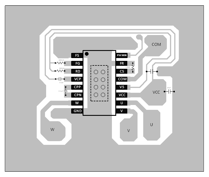
Figure 17. Layout Example Schematic