JAJSF51A April   2018  – July 2018 DRV8306

PRODUCTION DATA.  

  1. 特長
  2. アプリケーション
  3. 概要
    1.     概略回路図
  4. 改訂履歴
  5. 概要(続き)
  6. Pin Configuration and Functions
    1.     Pin Functions
  7. Specifications
    1. 7.1 Absolute Maximum Ratings
    2. 7.2 ESD Ratings
    3. 7.3 Recommended Operating Conditions
    4. 7.4 Thermal Information
    5. 7.5 Electrical Characteristics
    6. 7.6 Typical Characteristics
  8. Detailed Description
    1. 8.1 Overview
    2. 8.2 Functional Block Diagram
    3. 8.3 Feature Description
      1. 8.3.1 Three Phase Smart Gate Drivers
        1. 8.3.1.1 PWM Control Mode (1x PWM Mode)
        2. 8.3.1.2 Hardware Interface Mode
        3. 8.3.1.3 Gate Driver Voltage Supplies
        4. 8.3.1.4 Smart Gate Drive Architecture
          1. 8.3.1.4.1 IDRIVE: MOSFET Slew-Rate Control
          2. 8.3.1.4.2 TDRIVE: MOSFET Gate Drive Control
          3. 8.3.1.4.3 Gate Drive Clamp
          4. 8.3.1.4.4 Propagation Delay
          5. 8.3.1.4.5 MOSFET VDS Monitors
          6. 8.3.1.4.6 VDRAIN Sense Pin
      2. 8.3.2 DVDD Linear Voltage Regulator
      3. 8.3.3 Pulse-by-Pulse Current Limit
      4. 8.3.4 Hall Comparators
      5. 8.3.5 FGOUT Signal
      6. 8.3.6 Pin Diagrams
      7. 8.3.7 Gate-Driver Protective Circuits
        1. 8.3.7.1 VM Supply Undervoltage Lockout (UVLO)
        2. 8.3.7.2 VCP Charge-Pump Undervoltage Lockout (CPUV)
        3. 8.3.7.3 MOSFET VDS Overcurrent Protection (VDS_OCP)
        4. 8.3.7.4 VSENSE Overcurrent Protection (SEN_OCP)
        5. 8.3.7.5 Gate Driver Fault (GDF)
        6. 8.3.7.6 Thermal Shutdown (OTSD)
    4. 8.4 Device Functional Modes
      1. 8.4.1 Gate Driver Functional Modes
        1. 8.4.1.1 Sleep Mode
        2. 8.4.1.2 Operating Mode
        3. 8.4.1.3 Fault Reset (ENABLE Reset Pulse)
  9. Application and Implementation
    1. 9.1 Application Information
      1. 9.1.1 Hall Sensor Configuration and Connection
        1. 9.1.1.1 Typical Configuration
        2. 9.1.1.2 Open Drain Configuration
        3. 9.1.1.3 Series Configuration
        4. 9.1.1.4 Parallel Configuration
    2. 9.2 Typical Application
      1. 9.2.1 Primary Application
        1. 9.2.1.1 Design Requirements
        2. 9.2.1.2 Detailed Design Procedure
          1. 9.2.1.2.1 External MOSFET Support
            1. 9.2.1.2.1.1 Example
          2. 9.2.1.2.2 IDRIVE Configuration
            1. 9.2.1.2.2.1 Example
          3. 9.2.1.2.3 VDS Overcurrent Monitor Configuration
            1. 9.2.1.2.3.1 Example
        3. 9.2.1.3 Application Curves
  10. 10Power Supply Recommendations
    1. 10.1 Bulk Capacitance Sizing
  11. 11Layout
    1. 11.1 Layout Guidelines
    2. 11.2 Layout Example
  12. 12デバイスおよびドキュメントのサポート
    1. 12.1 デバイス・サポート
      1. 12.1.1 デバイスの項目表記
    2. 12.2 ドキュメントのサポート
      1. 12.2.1 関連資料
    3. 12.3 ドキュメントの更新通知を受け取る方法
    4. 12.4 コミュニティ・リソース
    5. 12.5 商標
    6. 12.6 静電気放電に関する注意事項
    7. 12.7 Glossary
  13. 13メカニカル、パッケージ、および注文情報

パッケージ・オプション

メカニカル・データ(パッケージ|ピン)
サーマルパッド・メカニカル・データ
発注情報

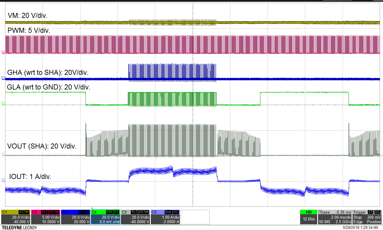
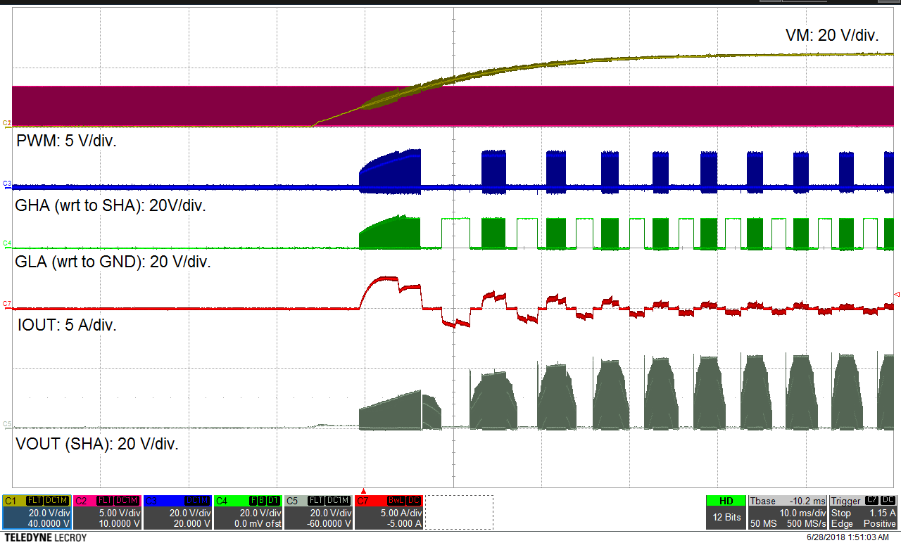
Application Curves

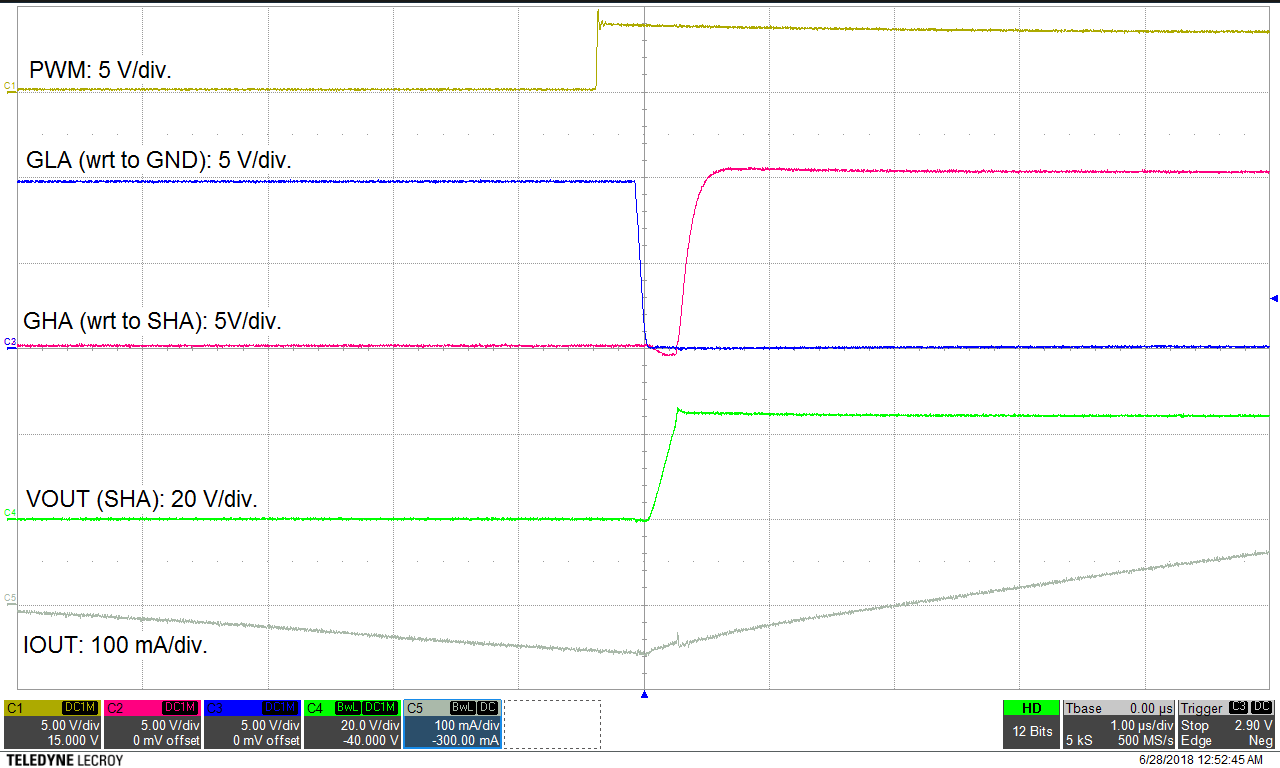
DRV8306 drv8306-idrive-maximum-setting-application-curve.pngFigure 31. IDRIVE Maximum Setting
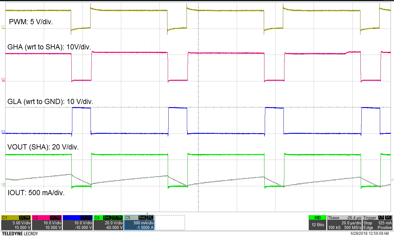
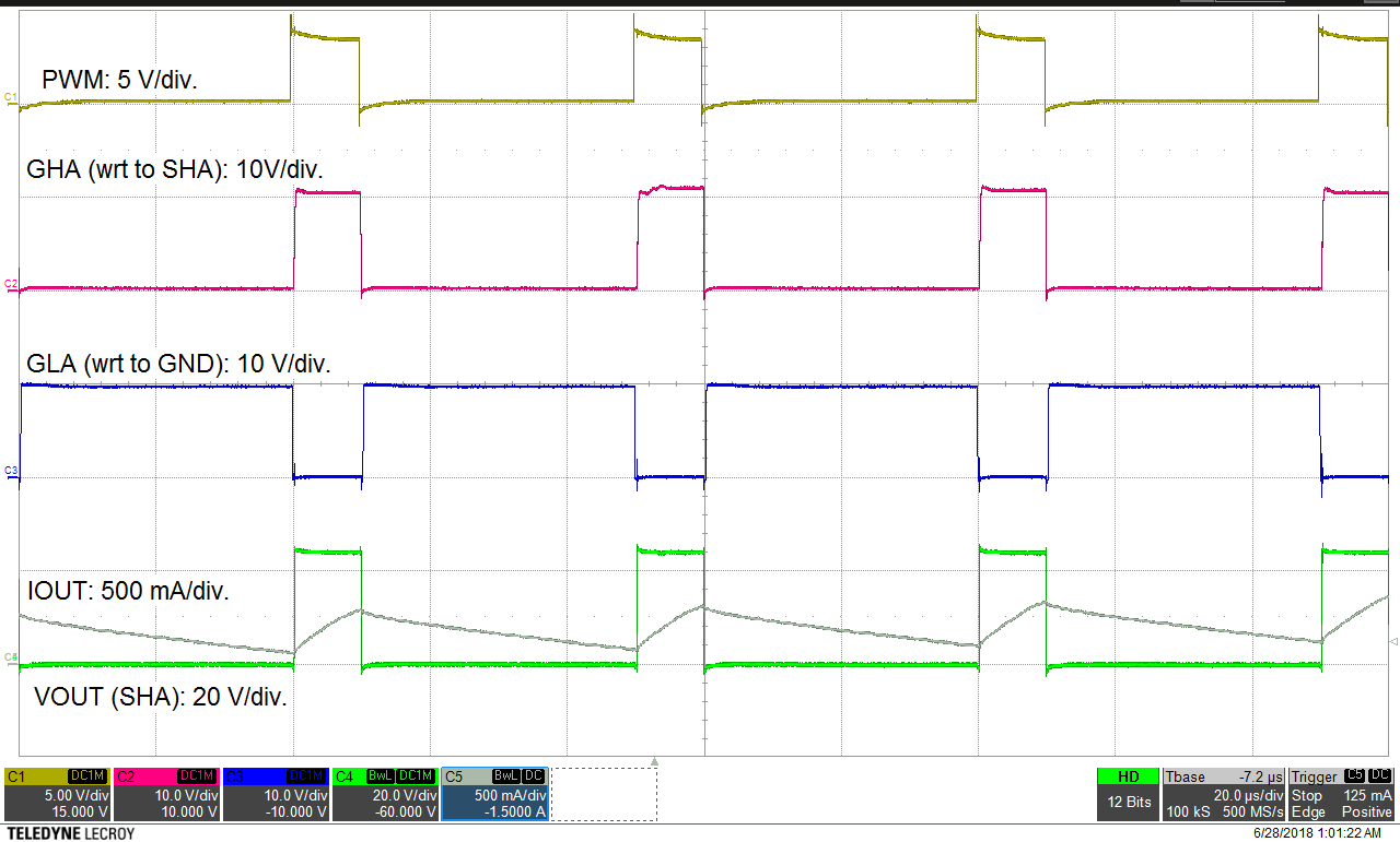
DRV8306 drv8306-gate-driver-80p-duty-cycle-application-curve.pngFigure 33. Gate Drive 80% Duty Cycle
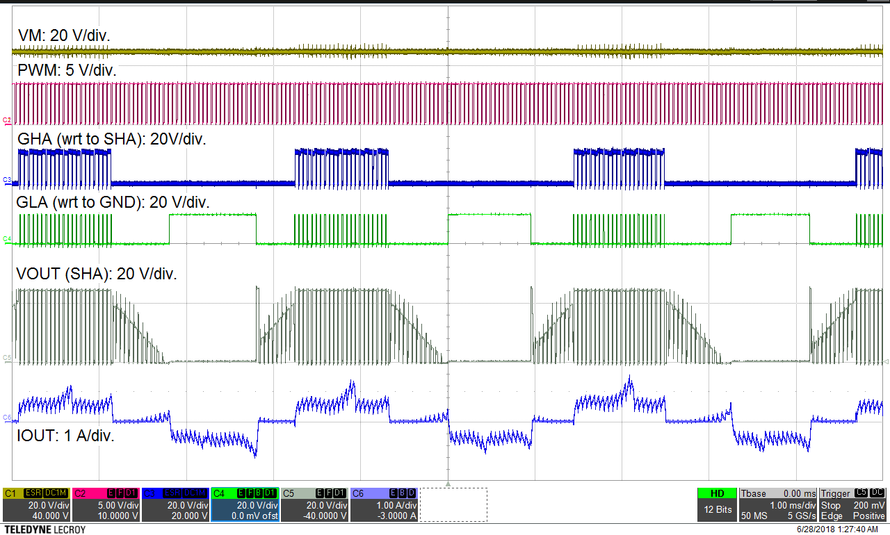
DRV8306 drv8306-motor-operation-at-80-percent-pwm-duty-application-curve.pngFigure 35. Motor Operation at 80% PWM Duty
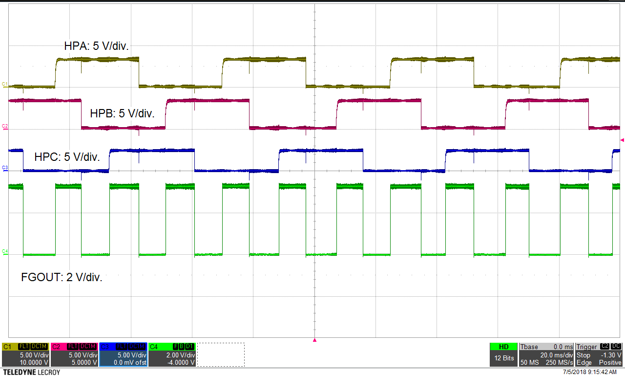
DRV8306 drv8306-hall-operation-application-curve.pngFigure 37. Hall Operation (Digital Hall Sensors Connected)
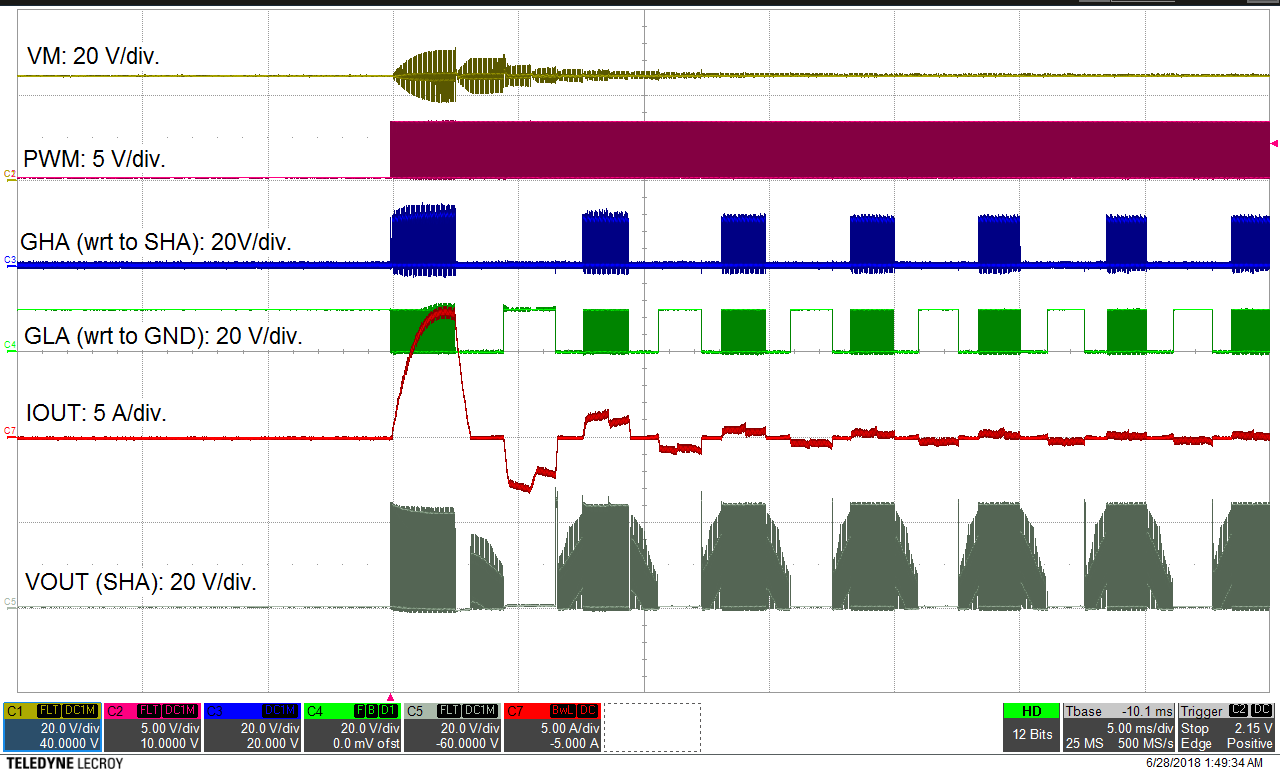
DRV8306 drv8306-motor-starting-with-pwm-duty-change-curve.pngFigure 39. Motor Starting With PWM Duty Change
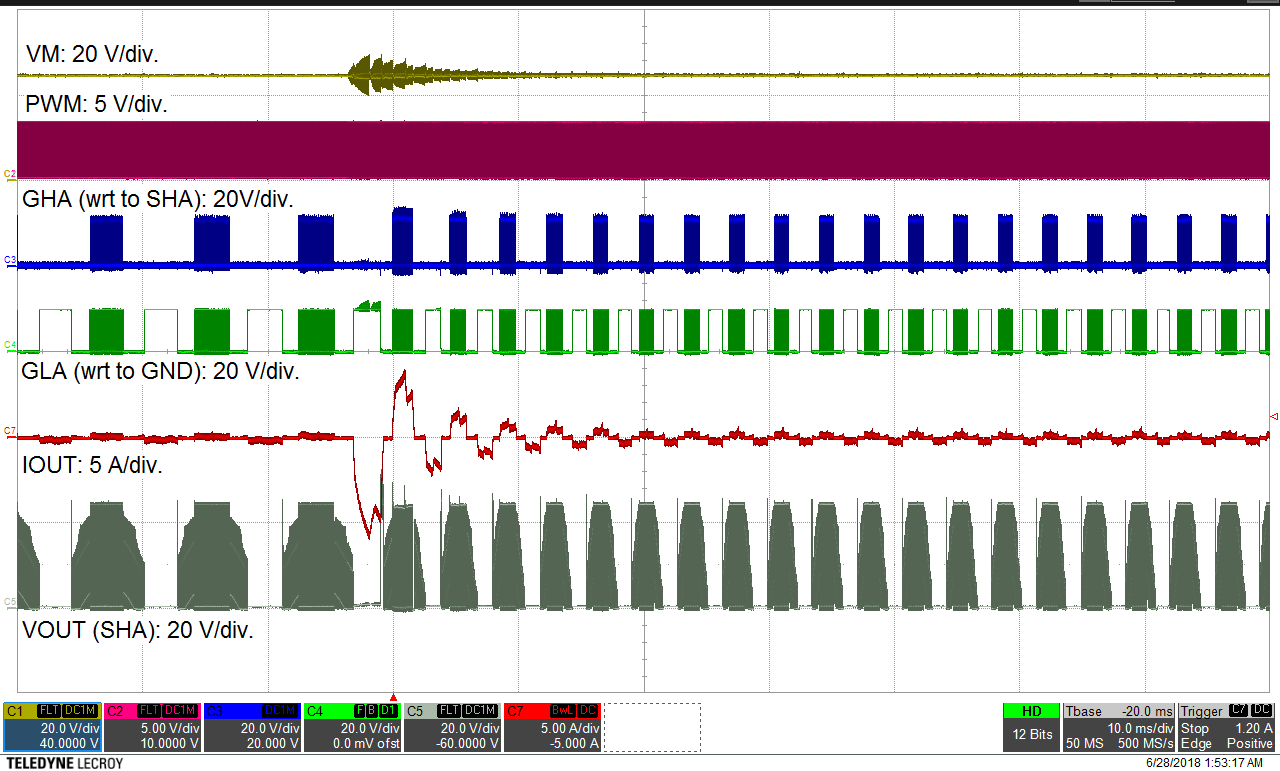
DRV8306 drv8306-motor-performance-at-speed-change-curve.pngFigure 41. Motor Performance at Speed Change
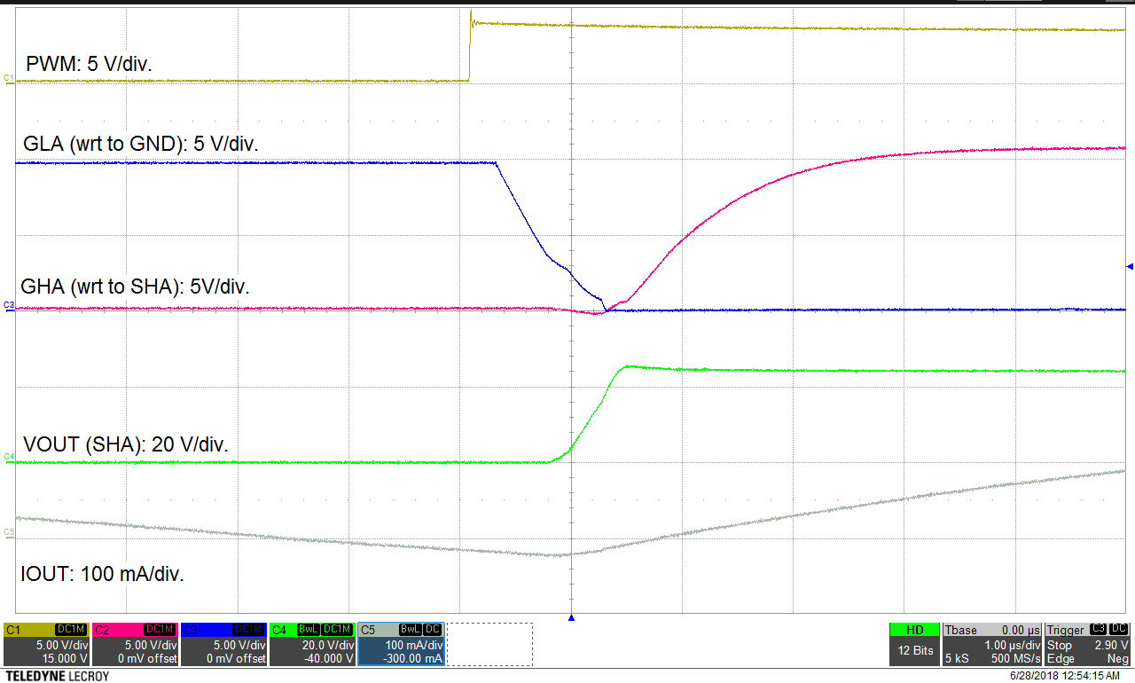
DRV8306 drv8306-idrive-minimum-setting-application-curve.pngFigure 32. IDRIVE Minimum Setting
DRV8306 drv8306-gate-driver-20p-duty-cycle-application-curve.pngFigure 34. Gate Drive 20% Duty Cycle
DRV8306 drv8306-motor-operation-at-20-percent-pwm-duty-application-curve.pngFigure 36. Motor Operation at 20% PWM Duty
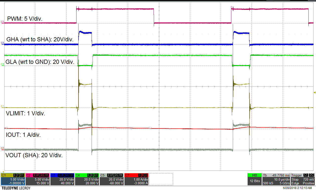
DRV8306 drv8306-vlimit-operation-application-curve.pngFigure 38. VLIMIT Operation
DRV8306 drv8306-motor-starting-with-supply-voltage-change-curve.pngFigure 40. Motor Starting With Supply Voltage Change
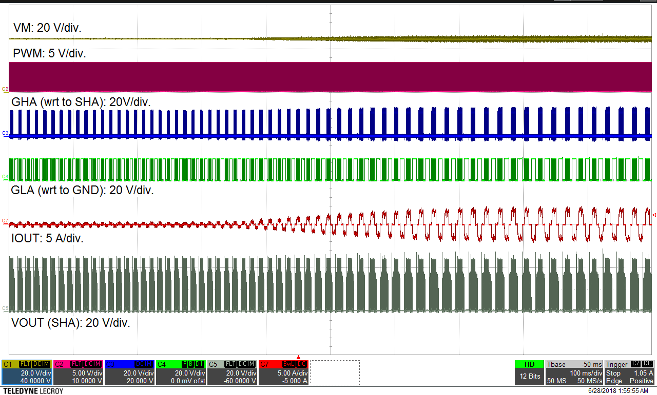
DRV8306 drv8306-motor-performance-at-load-change-curve.pngFigure 42. Motor Performance at Load Change